
Organic polymer film for OLED (organic light emitting diode) device film packaging and application of organic polymer film

A polymer film and film encapsulation technology, which is applied in the manufacture of electrical solid devices, semiconductor devices, semiconductor/solid devices, etc., can solve problems such as cracks and stress concentration of inorganic layers, achieve high transparency, improve flatness, and improve bending resistance The effect of foldability

Inactive Publication Date: 2019-10-11
ZHEJIANG HUADISPLAY OPTOELECTRONICS CO LTD
View PDF4 Cites 4 Cited by
  • Summary
  • Abstract
  • Description
  • Claims
  • Application Information

AI Technical Summary

Problems solved by technology

[0005] The purpose of the present invention is to provide a polymer film used for thin film packaging of OLED devices, which is used to solve the brittleness problems such as stress concentration and even cracks in the inorganic layer in the existing organic light emitting diode flexible film packaging

Method used


Image

  • Organic polymer film for OLED (organic light emitting diode) device film packaging and application of organic polymer film
  • Organic polymer film for OLED (organic light emitting diode) device film packaging and application of organic polymer film
  • Organic polymer film for OLED (organic light emitting diode) device film packaging and application of organic polymer film

Examples


Embodiment 1

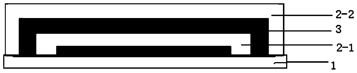
[0062] Transparent ITO substrates were ultrasonically cleaned in isopropanol for 15 min and exposed to UV light for 30 min, followed by plasma treatment for 10 min. Then put the processed ITO substrate into the evaporation equipment. Put monomers A, B and initiator TPO into three evaporation crucibles, and then evaporate 5 ± 2 μm organic monomer film on the substrate, wherein A accounts for 75% of the total weight of the initiator and photocurable monomer, and B It accounts for 22% of the total weight of the initiator and the photocurable monomer, and the IPO accounts for 3% of the total weight of the initiator and the photocurable monomer. Then it was cured under 100mJ / cm2 of ultraviolet radiation for 10min to make it solidified.

Embodiment 2

[0064] Transparent ITO substrates were ultrasonically cleaned in isopropanol for 15 min and exposed to UV light for 30 min, followed by plasma treatment for 10 min. Then put the processed ITO substrate into the evaporation equipment. Put monomers A, B and initiator TPO into three evaporation crucibles, and then evaporate 5 ± 2 μm organic monomer film on the substrate, wherein A accounts for 75% of the total weight of the initiator and photocurable monomer, and B Accounting for 22% of the total weight of the initiator and the photocurable monomer, TPO accounts for 3% of the total weight of the initiator and the photocurable monomer. Then it was cured under 500mJ / cm2 ultraviolet radiation for 10min to make it solidified.

Embodiment 3

[0066] Transparent ITO substrates were ultrasonically cleaned in isopropanol for 15 min and exposed to UV light for 30 min, followed by plasma treatment for 10 min. Then put the processed ITO substrate into the evaporation equipment. Put monomers A, B and initiator TPO into 3 evaporation crucibles respectively, and then evaporate a 5 ± 2 μm organic monomer film on the substrate, wherein A accounts for 75% of the total weight of the initiator and photocurable monomer, B accounts for 22% of the total weight of the initiator and the photocurable monomer, and TPO accounts for 3% of the total weight of the initiator and the photocurable monomer. Then it was cured under 1000mJ / cm2 ultraviolet radiation for 10min to make it solidified.


PUM

PropertyMeasurementUnit
Glass transition temperatureaaaaaaaaaa

Abstract

The invention discloses an organic polymer film for OLED (organic light emitting diode) device film packaging, belonging to the technical field of display panel packaging. The organic film is preparedfrom photocuring monomer (methyl) acrylate or a low polymer thereof through ultraviolet light curing reaction under the existence of a photoinitiator, and the structural general formula is that: theorganic polymer film solves the fragile problem that an inorganic layer generates stress concentration or even cracks easily in current flexible film packaging. The organic polymer film is applied onto an organic light emitting diode device, and comprises a baseplate, an organic light emitting diode deposited on the baseplate, an inorganic film packaging protection layer on the surface of the organic light emitting diode and an organic film protection layer stacked on the surface of an inorganic film. The organic polymer film used by the invention can prevent an OLED from destruction such as oxidation, reduction or degradation caused by factors such as oxygen and water in the environment, then the performance of an OLED lighting display device is improved, and the service life of the OLEDlighting display device is prolonged.

Description

technical field [0001] The invention relates to the field of display panel packaging, in particular to an organic polymer film used for thin film packaging of OLED devices. Background technique [0002] Organic electroluminescent devices (Organic Light-Emitting Diode, OLED) have a series of advantages such as self-luminescence, high brightness, high contrast, fast response speed, flexible preparation, low driving voltage, low power consumption, etc., in the future display, Lighting and other fields have very broad application prospects. However, the development of OLEDs still faces many challenges, the most critical of which is to solve the problem of device failure due to long-term exposure to air, water vapor and oxygen. Therefore, OLED devices need to be packaged, and the water oxygen transmission rate is required to be lower than 10 -6 g / m 2 d. [0003] OLED packaging technology has experienced traditional packaging, inorganic thin film packaging, organic thin film p...

Claims


Application Information

Patent Timeline
IPC IPC(8): C08L35/02C08J5/18C08F222/14C08F122/14C08F2/48H01L51/52
CPCC08J5/18C08F222/1006C08F2/48C08J2335/02C08F122/1006C08F222/103H10K50/844
Inventor 汪华月韩爱英
Owner ZHEJIANG HUADISPLAY OPTOELECTRONICS CO LTD
Features
  • Generate Ideas
  • Intellectual Property
  • Life Sciences
  • Materials
  • Tech Scout
  • Unparalleled Data Quality
  • Higher Quality Content
  • 60% Fewer Hallucinations
Learn More