Method for growing graphene on silicon substrate by using PEALD

A silicon substrate, graphene technology, applied in electrical components, semiconductor/solid-state device manufacturing, circuits, etc., can solve problems such as graphene defects, metal residues, slow migration speed, etc., to reduce the size of wrinkles and promote dehydrogenation Process, effect of good compatibility

Active Publication Date: 2019-10-11
ZHEJIANG UNIV
View PDF6 Cites 2 Cited by
  • Summary
  • Abstract
  • Description
  • Claims
  • Application Information

AI Technical Summary

Problems solved by technology

Using this method can only be based on copper substrates with good catalytic activity, and graphene must be transferred to the target substrate in order to achieve practical applications. The transfer process will inevitably cause defects in graphene, and there are problems such as metal residues. Seriously affect the performance of the prepared device, poor compatibility with the current silicon process
[0007] Due to the lack of catalytic activity, silicon itself cannot promote the cracking of organic precursors like transition metals, and the cracking of organic precursors is an endothermic reaction, and the temperature rise is conducive to the reaction. However, unlike metals, silicon can Under certain conditions, it will directly react with carbon to form a silicon carbide phase. Generally, there will be a large amount of silicon and carbon directly reacting above 900°C, so the growth of graphene on the silicon surface must be limited to below 900°C. dangling bonds interact with carbon-containing groups, resulting in low mobility and slow migration of carbon on the silicon surface, which directly affects the growth of graphene
Therefore, it has always been very difficult to grow graphene directly on the silicon surface. Using the conventional PEALD method, such as the PEALD technology disclosed in the above-mentioned patent specification, still cannot satisfy the growth of high-quality graphene.

Method used


Image

  • Method for growing graphene on silicon substrate by using PEALD
  • Method for growing graphene on silicon substrate by using PEALD
  • Method for growing graphene on silicon substrate by using PEALD

Examples


Embodiment 1

[0053] The method of utilizing PEALD of the present embodiment to grow graphene on a silicon substrate specifically comprises the steps:

[0054] (1) Take (100) silicon wafers for growth, place them in deionized water for simple ultrasonic cleaning for 1 min, and then immerse in dilute hydrofluoric acid with a volume ratio of 1:50 for 1 min.

[0055] (2) Take out the silicon wafer, rinse the surface with deionized water, and blow dry with 0.5MPa high-pressure nitrogen.

[0056] (3) Benzene is used as a carbon source, small oxygen-containing organic molecules are used as an auxiliary source, and high-purity hydrogen / argon gas mixture is used as a plasma gas source.

[0057] (4) The treated silicon wafer is placed in a tube furnace, evacuated to below 40mTorr, heated to 700°C under 50sccm argon gas and kept stable.

[0058] (5) Start the PEALD cycle, each cycle includes: pulse benzene or formic acid for 0.03 seconds, close the vacuum valve and react for 5 seconds, so that the s...

Embodiment 2

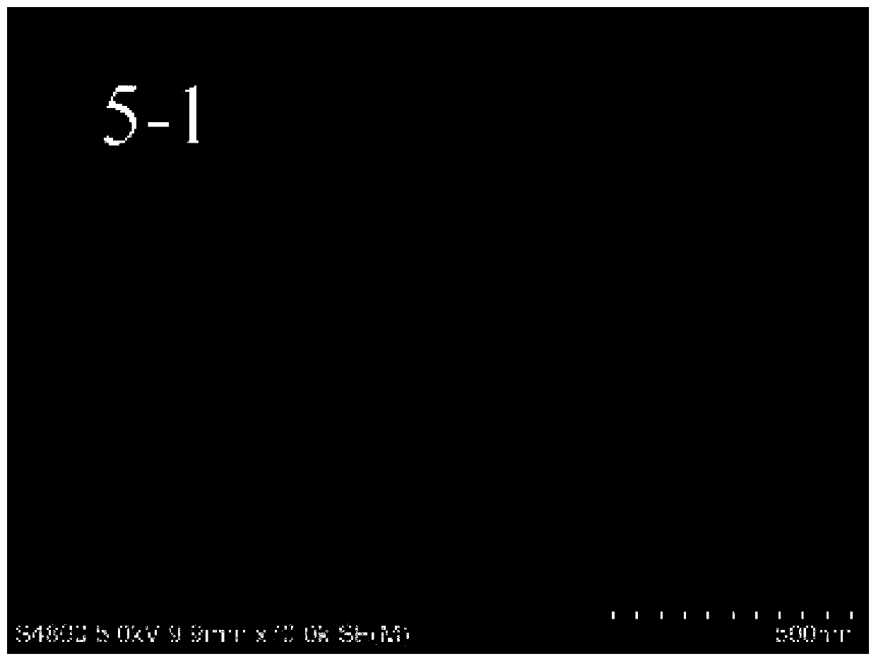
[0061] The difference with Example 1 is only that after every carbon source cycle is carried out 5 times, an auxiliary source cycle is carried out, which is denoted as 5-1, and the graphene grown on the silicon substrate is obtained. The graphene scanning electron microscope photo is as follows figure 2 shown.

Embodiment 3

[0063] The difference with Example 1 is only that after every 10 carbon source cycles, an auxiliary source cycle is carried out, denoted as 10-1, to obtain graphene grown on a silicon substrate, and the graphene scanning electron microscope photo is as follows image 3 shown.

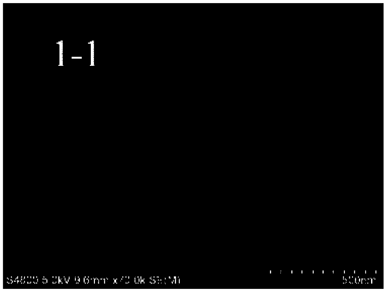
[0064] Compare figure 1 , 3 , 4, it can be seen that figure 1 The protrusions on the surface of graphene are mostly island-shaped, and the size is small, and there are no large linear folds. Compared with Figure 4 The growth morphology of Example 3 is significantly different, which proves that the use of formic acid as an auxiliary source can improve the quality of growth.

[0065] With the increase of the amount of formic acid, the wrinkles on the graphene surface were significantly reduced. This is because oxygen plays a role in assisting the dehydrogenation of benzene during the reaction process, which is conducive to the growth of graphene in the uncovered area, thereby reducing wrinkles and mu...


PUM


Abstract

The invention discloses a method for growing graphene on a silicon substrate by using PEALD. The clean silicon substrate is placed in a reaction chamber for carrying out PEALD cycles, and each cycle comprises the following steps: (1) carrying out adsorption of a carbon source or an auxiliary source, wherein the carbon source is selected from at least one of benzene series and methane, and the auxiliary source is an oxygen-containing organic matter; (2) cleaning the adsorbed silicon substrate, and carrying out plasma pulse; and (3) cleaning the silicon substrate after plasma pulse. According tothe method, graphene can be grown on the silicon substrate in a large area, and has good compatibility with a current silicon-based semiconductor technology. According to the method, growth is promoted by using oxygen-containing small molecules, on one hand, vacancy-type defects are compensated by taking graphene as small molecular carbon, the D peak of a defect peak after the reaction is reduced, on the other hand, the participation of oxygen element promotes a dehydrogenation process of benzene in the growth process, the size of wrinkles after film formation is reduced, and the quality of large-area grown graphene through atomic layer deposition and growth on the silicon substrate is improved.

Description

technical field [0001] The invention relates to the technical field of graphene functional material preparation, in particular to a method for growing graphene on a silicon substrate by using PEALD. Background technique [0002] As the core material in the semiconductor field, silicon materials are particularly concerned about its photoelectric properties. Limited by the indirect bandgap structure of intrinsic silicon, the photoelectric conversion capability of silicon itself is not excellent. Therefore, the optoelectronic properties of composite structures of silicon materials and new materials have become a research hotspot in recent years. For the integrated circuit (IC) industry, the current state-of-the-art technology has reached a theoretical 7nm line width, and as the gate width narrows, the resistance on the line becomes very large. Various chip design companies hope to obtain higher performance, lower power consumption and smaller chip area through process upgrade...

Claims


Application Information

Patent Timeline
IPC IPC(8): H01L21/02
CPCH01L21/02381H01L21/02527H01L21/0262
Inventor 余学功丛靖昆黄琨杨德仁
Owner ZHEJIANG UNIV
Why Eureka
Try Eureka