Supercharge Your Innovation With Domain-Expert AI Agents!

Plasma treatment method and plasma treatment device

A processing method and processing device technology, applied in the direction of measuring devices, optical devices, instruments, etc., to achieve good reproducible results

Active Publication Date: 2019-10-11
HITACHI HIGH-TECH CORP
View PDF5 Cites 4 Cited by
  • Summary
  • Abstract
  • Description
  • Claims
  • Application Information

AI Technical Summary

Problems solved by technology

However, in such cyclic etching using a gas with high accumulation property, it is necessary to precisely control etching parameters such as the amount of deposition in the deposition process and the ion energy in the etching process to perform etching. The atmosphere changes with time, etc., it is difficult to control the deposition process and etching process stably for a long time to etch into the desired shape

Method used


Image

  • Plasma treatment method and plasma treatment device
  • Plasma treatment method and plasma treatment device
  • Plasma treatment method and plasma treatment device

Examples


Embodiment 1

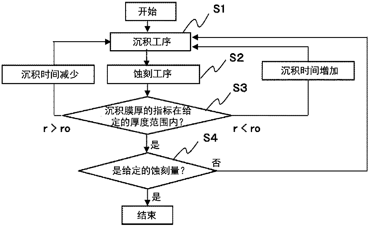
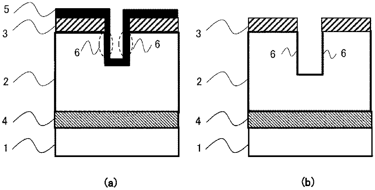
[0037] As Example 1, an example of a cyclic etching and etching apparatus that performs deposition steps and etching steps alternately to process fine patterns will be described. figure 1 It is a figure which shows an example of the process flow of the cyclic etching including several steps (S) concerning Example 1. figure 2 is for illustration figure 1 A schematic diagram of the process flow, figure 2 (a) is an explanatory diagram of a deposition process (S1), and (b) is an explanatory diagram of an etching process (S2). In this embodiment, as an example of the pattern to be etched, the following case is described: a non-etching layer 4 and an interlayer film of the material to be etched 2 are formed on the wafer 1 as the substrate to be etched, and the pattern to be etched is formed on the mask 3, i.e. A fine line and space pattern, in this case, etches the material 2 to be etched. In addition, in this embodiment, a case where etching is performed using energy of ions i...

Embodiment 2

[0070] Next, use Figure 11 A plasma processing apparatus comprising a cluster type etching tool (hereinafter referred to as a cluster tool) according to Example 2 will be described. Figure 11 It is a figure which shows one structure of the cluster tool of Example 2. As an example of this cluster tool, the case where the processing chamber of the etching apparatus is composed of three chambers is shown. The cluster tool includes a cassette loader 204 , a control PC 205 , a transport robot 207 , a control unit 220 , and a notch position adjustment table 221 in addition to three processing chambers. In the structure of this embodiment, the PC for control, the control part 220, and the three monitor control parts 36 can be collectively called the control part of a cluster tool.

[0071] In this cluster of tools, if the wafer cassette is placed on the wafer loader 204, the wafer 1 for processing is transported from the wafer cassette to the notch position matching process by th...


PUM


Abstract

According to the present invention, a desired shape is etched by means of highly-precise control and long-term stabilization of the thickness of a film that is deposited on a pattern during cyclical etching that proceeds by the repetition of a deposition step and an etching step. The present invention comprises: a deposition step (S1) for introducing a reactive, depositing gas into a treatment chamber to form a deposit layer on the surface of an etching pattern of an etching substrate; an etching step (S2) for removing the product of a reaction between the deposit layer and the surface of theetching pattern; and a step (S3) for shining light onto the etching pattern during the deposition steps that form the deposit layer during cyclical etching in which the deposition step and the etchingstep are alternatingly executed to produce a fine pattern and monitoring the change in the film thickness of the deposit layer on the basis of the change in interference light of a specific wavelength that has been reflected by the etching pattern. Treatment conditions for the steps that will form the deposit layer during subsequent cycles of the cyclical etching are determined such that a deposited film thickness index that is calculated from the monitored change in the film thickness of the deposit layer falls within a prescribed range in comparison with reference data.

Description

technical field [0001] The present invention relates to a plasma processing method and a plasma processing device, and particularly to a plasma etching technique suitable for controlling the thickness of a deposited film on a pattern. Background technique [0002] Due to the miniaturization of functional device products such as semiconductor devices, the development of device processing technologies using multiple patterning such as double patterning using the side walls of the partition walls of thin films as masks is accelerating. [0003] Along with this, in the process of processing devices such as three-dimensional devices, the technology of trench processing using various insulating materials such as film partition walls as a mask has become important. Thicknesses of masks, gate insulating films, etching stoppers, etc. are reduced, and highly selective processing that controls shapes at the atomic layer level is required. In addition, with the three-dimensionalization...

Claims


Application Information

Patent Timeline
Patent Type & Authority Applications(China)
IPC IPC(8): H01L21/3065
CPCH01J37/32082H01J37/32963H01J37/32715H01L22/26H01L22/12H01L21/67167H01L21/67207G01B11/065H01L21/31116H01L21/3065H01L21/67069H01L21/67242H01L21/30655H01L21/308H01J2237/24578H01L21/67253G01B11/0625H01J2237/3347H01J2237/332
Inventor 松井都臼井建人伊泽胜桑原谦一
Owner HITACHI HIGH-TECH CORP
Features
  • R&D
  • Intellectual Property
  • Life Sciences
  • Materials
  • Tech Scout
  • Unparalleled Data Quality
  • Higher Quality Content
  • 60% Fewer Hallucinations
Learn More