Device and method for preparing or treating auxiliary film aided by pulse electric field

A technology of film treatment and treatment method, applied in the field of exploring film materials, can solve the problems of slow cooling, slow heating and performance degradation

Active Publication Date: 2019-10-18
NORTHEASTERN UNIV
View PDF3 Cites 1 Cited by
  • Summary
  • Abstract
  • Description
  • Claims
  • Application Information

AI Technical Summary

Problems solved by technology

In the current process of preparing thin films, physical vapor deposition equipment has problems such as slow temperature rise and slow temperature drop.
At the same time, since the performance of the material will decrease after the material is reduced in dimension, how to optimize the performance of the thin film material has become the focus and difficulty of research.

Method used


Image

  • Device and method for preparing or treating auxiliary film aided by pulse electric field
  • Device and method for preparing or treating auxiliary film aided by pulse electric field
  • Device and method for preparing or treating auxiliary film aided by pulse electric field

Examples


Embodiment 1

[0057] Preparation of TiAlN coating under pulsed electric field

[0058] Step 1, cleaning of the substrate

[0059] After grinding and polishing the cemented carbide sheet, use acetone and alcohol to ultrasonically clean the sapphire substrate for 15 minutes. After cleaning, use high-purity inert gas to dry it. Use a pulse electric field clamp to fix the substrate and put it into a vacuum chamber.

[0060] Step 2, preparation of TiAlN coating under pulsed electric field

[0061] Using the same preparation conditions as in Comparative Example 1, a pulse current was connected during the preparation process to prepare a TiAlN coating under a pulse electric field. Among them, the pulse current intensity is 15A, the pulse width is 10s, and the processing time is 5-10min.

[0062] Step 3, turn off the magnetron sputtering equipment, take out the sample after degassing, put it into a centrifuge tube, and inject inert high-purity Ar for subsequent detection.

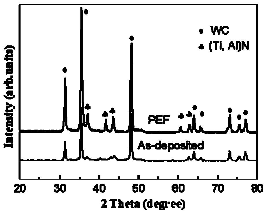
[0063] figure 1 XRD ...

Embodiment 2

[0078] Oxidation Treatment of Ca-Co Thin Films Using Pulse Electric Field

[0079] Step 1, connect the circuit

[0080] Use a clamp to fix the film, and connect the clamp and the pulse current generator to form a closed loop.

[0081] Step 2, pulsed electric field oxidation treatment of Ca-Co film

[0082] After setting the pulse electric field pulse current 0.01A, pulse width 1s, pulse rise time 0.05A / s and other parameters, start processing, processing time 1h.

[0083] Step 3, end of processing, take out the sample

[0084] After the timing is over, the sample is taken out, put into a centrifuge tube, and passed through inert high-purity Ar for subsequent detection.

[0085] Figure 6 It is a comparison chart of the XRD diffraction pattern of Co-Ca in Example 2 when it is oxidized by a pulsed electric field and Comparative Example 3 when it is oxidized by a tube furnace.

[0086] From the XRD diffraction pattern, it can be found that the Co-Ca compound can be oxidized ...

Embodiment 3

[0096] Pulsed electric field heat treatment of Bi 2 Te 3 film

[0097] Step 1, connect the circuit

[0098] Use a clamp to fix the film, and connect the clamp and the pulse current generator to form a closed loop. Fix the thermocouple above the film and connect the temperature collector to the display.

[0099] Step 2, pulsed electric field heat treatment of Bi 2 Te 3 film

[0100] After setting the pulse electric field pulse current 0.05A, pulse width 1s, pulse rise time 0.05A / s and other parameters, start processing, processing time 1h, and collect temperature changes at the same time.

[0101] Step 3, end of processing, take out the sample

[0102] After the timing is over, the sample is taken out, put into a centrifuge tube, and passed through inert high-purity Ar for subsequent detection.

[0103] Figure 8 Deposited Bi prepared for Comparative Example 4 2 Te 3 Film and the Bi after pulse electric field heat treatment of embodiment 3 2 Te 3 SEM comparison ima...


PUM

PropertyMeasurementUnit
dispersion coefficientaaaaaaaaaa

Abstract

The invention provides a device and a method for preparing or treating an auxiliary film aided by a pulse electric field. A thin film material is prepared below the pulse electric field. The preparation method is characterized in that a physical vapor deposition method is combined with the pulsed electric field, and the joule heat effect generated under the pulsed electric field is utilized to replace a traditional heating mode; the thin film material is oxidized in the pulsed electric field, the treatment mode is that oxidation treatment of the thin film material can be realized under the atmospheric condition, the treatment time is short, the temperature requirement is low, and a vacuum high-oxygen environment is not required to be realized; and the thin film material is subject to heattreatment by the pulse electric field, and the pulse electric field formed by the pulse current generator is used for carrying out heat treatment on the prepared electric thin film. When the pulsed electric field is used for preparing the thin film material, the pulse electric field can be instantly heated and cooled, so that the microstructure and the performance of the thin film are changed in the preparation process.

Description

technical field [0001] The invention belongs to the field of exploring thin film materials, and in particular relates to a device and method for preparing or processing thin films by using a pulsed electric field. Background technique [0002] Due to the rapid development of information, biotechnology, energy, environment, national defense and other industries, the size requirements of devices are getting smaller and smaller, and the requirements for material performance are getting higher and higher. Therefore, the research on low-dimensional thin film materials has entered a new stage. Because thin film materials can not only improve economic benefits, but also have very important significance for saving resources and energy, developing new functions of materials, improving reliability, and realizing light and thin. In the current process of preparing thin films, physical vapor deposition equipment has problems such as slow temperature rise and slow temperature drop. At ...

Claims


Application Information

Patent Timeline
Patent Type & Authority Applications(China)
IPC IPC(8): C23C14/35C23C14/58
CPCC23C14/3485C23C14/35C23C14/5806C23C14/5853
Inventor 李国建兰明迪刘诗莹刘晓明吕汶璋王强
Owner NORTHEASTERN UNIV
Why Eureka
Try Eureka