Ultraviolet photoelectric detector and preparation method thereof
A technology of electrical detectors and ultraviolet light, which is applied in the direction of circuits, electrical components, semiconductor devices, etc., can solve the problems of reducing carrier mobility and photoresponse speed, unfavorable perovskite thin films, and difficult material synthesis, etc., to achieve current-carrying The effect of long diffusion distance, fast carrier transport, and large grain size
- Summary
- Abstract
- Description
- Claims
- Application Information
AI Technical Summary
Problems solved by technology
Method used
Image

Examples
preparation example Construction
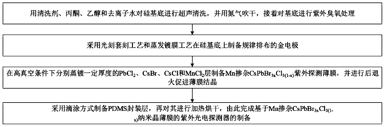
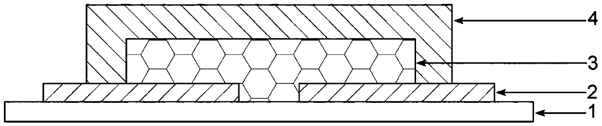
[0029] see figure 1 , the preparation method of the ultraviolet photodetector provided by the preferred embodiment of the present invention mainly includes the following steps:
[0030] Step 1, providing a silicon substrate with a silicon nitride insulating layer, and cleaning the silicon substrate.
[0031] Specifically, a silicon substrate with a silicon nitride insulating layer is provided, and the silicon substrate is ultrasonically cleaned with detergent, acetone, ethanol, and deionized water for 15 to 20 minutes; Blow dry, and then treat the silicon substrate with ultraviolet and ozone for 15-30 minutes.
[0032] Step 2, preparing an electrode layer on the silicon substrate by using a photolithographic overlay process and an evaporation coating process.
[0033] Specifically, an electrode layer is prepared on the silicon substrate by using a photolithographic overlay process and an evaporation coating process, the electrodes of the electrode layer are regularly arrange...
Embodiment 1
[0041] The preparation method of the ultraviolet photodetector provided by the first embodiment of the present invention mainly includes the following steps:
[0042] S1, providing a silicon substrate with a silicon nitride insulating layer, and cleaning the silicon substrate.
[0043] Specifically, a silicon substrate with a silicon nitride insulating layer is provided, and the silicon substrate is ultrasonically cleaned with detergent, acetone, ethanol, and deionized water for 15 minutes; then, the silicon substrate is blown dry with nitrogen gas flow , and then UV-ozone treatment was performed on the silicon substrate for 15 minutes.
[0044] S2, preparing an electrode layer on the silicon substrate by using a photolithographic overlay process and an evaporation coating process.
[0045] Specifically, an electrode layer was prepared on the silicon substrate by using a photolithographic overlay process and an evaporation coating process. The electrodes of the electrode laye...
Embodiment 2
[0052] The preparation method of the ultraviolet photodetector provided by the second embodiment of the present invention mainly includes the following steps:
[0053] B1, providing a silicon substrate with a silicon nitride insulating layer, and cleaning the silicon substrate.
[0054] Specifically, a silicon substrate with a silicon nitride insulating layer is provided, and the silicon substrate is ultrasonically cleaned with detergent, acetone, ethanol, and deionized water for 20 minutes; then, the silicon substrate is blown dry with nitrogen gas flow , and then UV-ozone treatment was performed on the silicon substrate for 30 minutes.
[0055] B2, preparing an electrode layer on the silicon substrate by using a photolithographic overlay process and an evaporation coating process.
[0056] Specifically, an electrode layer is prepared on the silicon substrate by using a photolithographic overlay process and an evaporation coating process, the electrodes of the electrode laye...
PUM
| Property | Measurement | Unit |
|---|---|---|
| thickness | aaaaa | aaaaa |
| thickness | aaaaa | aaaaa |
| thickness | aaaaa | aaaaa |
Abstract
Description
Claims
Application Information
 - R&D
- Intellectual Property
- Life Sciences
- Materials
- Tech Scout
- Unparalleled Data Quality
- Higher Quality Content
- 60% Fewer Hallucinations
Browse by: Latest US Patents, China's latest patents, Technical Efficacy Thesaurus, Application Domain, Technology Topic, Popular Technical Reports.
© 2025 PatSnap. All rights reserved.Legal|Privacy policy|Modern Slavery Act Transparency Statement|Sitemap|About US| Contact US: help@patsnap.com