High-speed superconductive nanowire single-photon detector integrating impedance matching structure
A single-photon detector and superconducting nanowire technology, which is used in photometry, photometry, and optical radiation measurement using electrical radiation detectors to achieve the effects of reducing noise, increasing rising edge slope, and increasing kinetic energy inductance.
- Summary
- Abstract
- Description
- Claims
- Application Information
AI Technical Summary
Problems solved by technology
Method used
Image
Examples
Embodiment 1
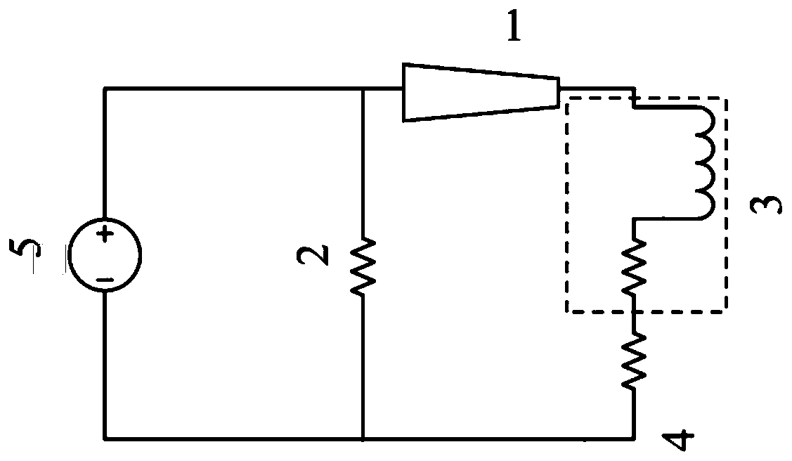
[0035] Light enters the closed-cycle refrigerator through a single-mode fiber, and is received by a single-photon detector through a fiber focuser. The anode of the single photon detector is connected to the high impedance end of the impedance matching structure, the cathode is connected to the 150 ohm resistor 4, and the other end of the ohm resistor 4 is grounded. The low impedance end of the impedance matching structure is connected with the current source 5 and the load 2 .
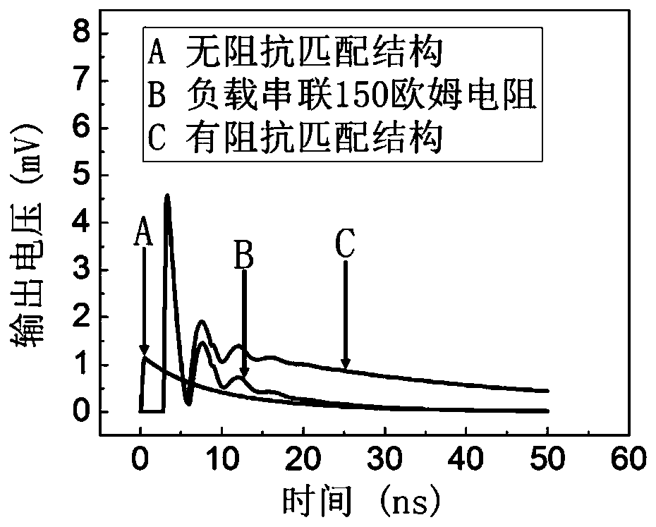
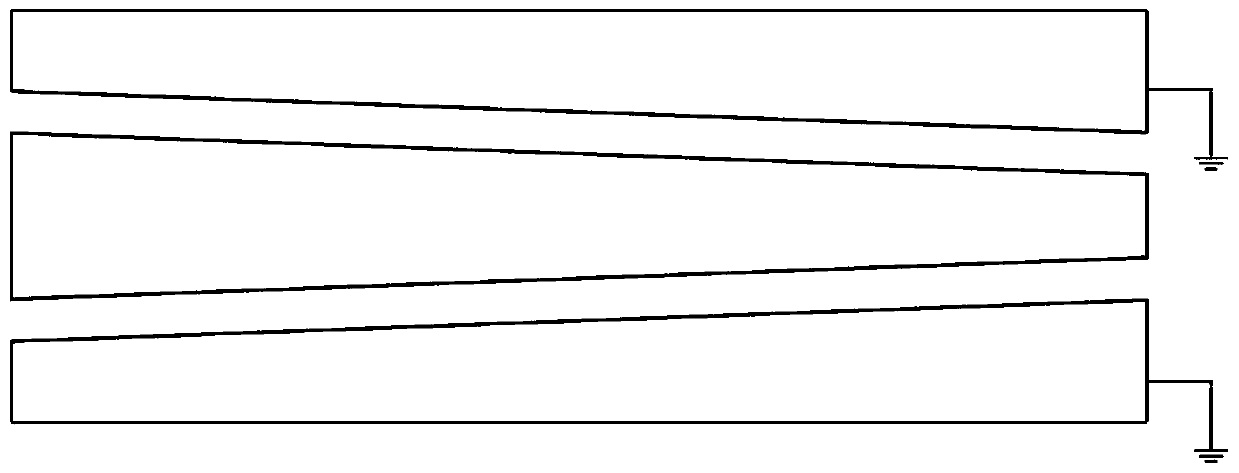
[0036] When a photon is incident on the single photon detector, the superconducting nanowire 3 changes from a superconducting state to a resistance state, forming a voltage pulse, and forming an output voltage through the transmission line. The impedance matching structure is high-pass, and acts as a transformer on the rising edge of the voltage pulse, that is, when the high-frequency signal passes through. Compared with the readout circuit of the traditional superconducting nanowire single photon det...
Embodiment 2
[0039] The impedance matching structure and the processing of the ohmic resistor 4:
[0040] A layer of titanium niobium nitride material with a thickness of about 9 nm is sputtered on the substrate by means of magnetron sputtering;
[0041] The nanowire pattern is transferred to the electron beam exposure glue by electron beam exposure method, and the electron beam exposure glue is used as a mask, and the nanowire pattern is etched by reactive ion beam etching method;
[0042] Through the method of photolithography-reactive ion beam etching-removing glue, use photoresist as a mask to dig out rectangular grooves on the niobium nitride film;
[0043] Deposit a strip-shaped titanium resistor at the trench by photolithography-electron beam evaporation-stripping method;
[0044] By means of photolithography-electron beam evaporation-stripping, a gold electrode aligned with the titanium resistor is deposited on the superconducting film, and the titanium resistor partially overlaps...
PUM
 Abstract
Description
Claims
Application Information


