Method for preparing thick film silicon nitride waveguide

A silicon nitride and waveguide technology, applied in the field of integrated optics, can solve problems such as rough side walls and poor waveguide shapes, and achieve the effects of optimizing waveguide shape and side wall roughness, avoiding unevenness, and solving high stress problems

Active Publication Date: 2019-11-15
INST OF MICROELECTRONICS CHINESE ACAD OF SCI
View PDF6 Cites 5 Cited by
  • Summary
  • Abstract
  • Description
  • Claims
  • Application Information

AI Technical Summary

Problems solved by technology

However, the problem of high stress in the growth of thick film silicon nitride has not been well solved. In addition, in the traditional trenching method, there will be many cavities, the shape of the waveguide is not good enough, and the sidewall is rough.

Method used


Image

  • Method for preparing thick film silicon nitride waveguide
  • Method for preparing thick film silicon nitride waveguide
  • Method for preparing thick film silicon nitride waveguide

Examples


preparation example Construction

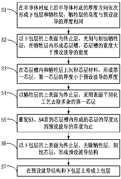
[0026] A method for preparing a thick-film silicon nitride waveguide in this embodiment, such as figure 1 shown, including:

[0027] S1, sequentially forming a lower cladding layer and a sacrificial layer on the semiconductor substrate along the thickness direction of the semiconductor substrate, and the height of the sacrificial layer is the same as the thickness of the predetermined waveguide;

[0028] On the basis of the above solutions, further, the semiconductor substrate in this implementation manner is a silicon substrate, and in other implementation manners, the semiconductor substrate may also be a quartz substrate.

[0029] On the basis of the above scheme, further, the lower cladding layer is formed by depositing a solid cladding material with a refractive index lower than 1.7 and higher than 1 by thermal oxidation or / and chemical vapor deposition; in other embodiments, the lower cladding layer can also be Formed by physical vapor deposition process. In some embod...

Embodiment 1

[0050] S1, sequentially forming a lower cladding layer and a sacrificial layer on the semiconductor substrate along the thickness direction of the semiconductor substrate, and the height of the sacrificial layer is the same as the thickness of the preset waveguide;

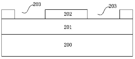
[0051]As shown in FIG. 2 ( 1 ), those skilled in the art can deposit and form the lower cladding layer 201 by thermal oxidation or / and chemical vapor deposition. Wherein, the material of the lower cladding layer 201 can be a solid cladding material with a refractive index lower than 1.7 and higher than 1, silicon dioxide or others, and the material used for the lower cladding layer 201 in this embodiment is preferably silicon dioxide; the sacrificial layer 202 adopts a deposition process, and the material used for the sacrificial layer 202 is preferably amorphous silicon; the material of the semiconductor substrate 200 can be a silicon substrate or a quartz substrate, and the material used for the semiconductor sub...

Embodiment 2

[0067] Compared with embodiment 1, step 1 to step 5 in embodiment 2 are identical with embodiment 1;

[0068] S6. The upper surface of the lower cladding layer is used as a termination layer, the sacrificial layer is removed, and the core layer is etched to form a preset waveguide structure;

[0069] As shown in FIG. 2 ( 11 ), the specific operation is to remove the sacrificial layer 202 by wet etching. Wherein, the process steps of the wet etching are as follows: the wet etching solution is determined according to the ratio of the amorphous silicon in the sacrificial layer 202 to the silicon dioxide in the lower cladding layer 201 . Specifically, a dilute tetramethylammonium hydroxide (TMAH) solution is used for wet etching. The etching rate of the selected wet etching solution to amorphous silicon is greater than that of silicon dioxide and silicon nitride, so that while removing the remaining sacrificial layer 202, no or only a small amount of core Layer 206.

[0070] As...


PUM

PropertyMeasurementUnit
thicknessaaaaaaaaaa
widthaaaaaaaaaa
widthaaaaaaaaaa

Abstract

The invention discloses a method for preparing a thick film silicon nitride waveguide, comprising the steps of: sequentially forming a lower cladding layer and a sacrificial layer on a semiconductor substrate, wherein the height of the sacrificial layer is the same as the thickness of a preset waveguide; photoetching and etching the sacrificial layer to form a core layer groove by using an upper surface of the lower cladding layer as a termination layer, wherein the width of the core layer groove is greater than the width of the preset waveguide; depositing a core layer material in the core layer groove and on the sacrificial layer to form a first core layer; removing the excess first core layer by using a surface planarization process and by using the upper surface of the sacrificial layer as the termination layer; repeating the above step until the thickness of the core layer formed in the core layer groove reaches the thickness of the preset waveguide; removing the sacrificial layerand etching the core layer to form a preset waveguide structure by using the upper surface of the lower cladding layer as the termination layer; and forming an upper cladding layer on the preset waveguide structure on the lower cladding layer. By adopting the scheme, the high stress problem caused by the excess thickness of the thin film is solved, and the shape of the waveguide is optimized to reduce the sidewall roughness.

Description

technical field [0001] The invention relates to the technical field of integrated optics, in particular to a method for preparing a thick-film silicon nitride waveguide. Background technique [0002] At present, the silicon nitride film growth and preparation methods mainly include LPCVD (low pressure chemical vapor deposition) and so on. The silicon nitride film deposited by LPCVD has good quality and low waveguide loss. However, when the thickness of the film is greater than 300 nanometers, due to the difference in thermal expansion coefficient between the film and the substrate, when the film grows in a large area, there will be a large stress and cracks will easily occur, thereby affecting the performance of the device. In the existing production process, a dry etching process is usually used to open a groove in the silicon dioxide cladding layer, and then fill the groove with silicon nitride to obtain a thick-film silicon nitride optical waveguide. However, the proble...

Claims


Application Information

Patent Timeline
Patent Type & Authority Applications(China)
IPC IPC(8): G02B6/13G02B6/132G02B6/136
CPCG02B6/13G02B6/132G02B6/136
Inventor 李彬李志华唐波
Owner INST OF MICROELECTRONICS CHINESE ACAD OF SCI
Why Eureka
Try Eureka