Multi-channel total-silicon-based infrared thermoelectric detector and manufacturing method thereof

A technology of pyroelectric detectors and manufacturing methods, which is applied in the field of photoelectric detection, can solve problems such as low quantum efficiency and detection rate, inability to work with silicon materials, and high dark current, and achieve the effects of improving photocurrent, perfect absorption, and high absorption rate

Inactive Publication Date: 2019-11-19
FUDAN UNIV
View PDF4 Cites 7 Cited by
  • Summary
  • Abstract
  • Description
  • Claims
  • Application Information

AI Technical Summary

Problems solved by technology

[0005] The purpose of the present invention is to propose a multi-channel all-silicon-based infrared photodetector structure and its manufacturing method to solve the problem that silicon materials cannot work due to the band gap limitation and the wave band greater than 1.1 μm, and overcome the responsivity of current silicon-based thermal electron infrared devices , low quantum efficiency and detection rate, and high dark current defects, to achieve high-sensitivity infrared monitoring capabilities of all-silicon photodetectors

Method used


Image

  • Multi-channel total-silicon-based infrared thermoelectric detector and manufacturing method thereof
  • Multi-channel total-silicon-based infrared thermoelectric detector and manufacturing method thereof
  • Multi-channel total-silicon-based infrared thermoelectric detector and manufacturing method thereof

Examples


Embodiment Construction

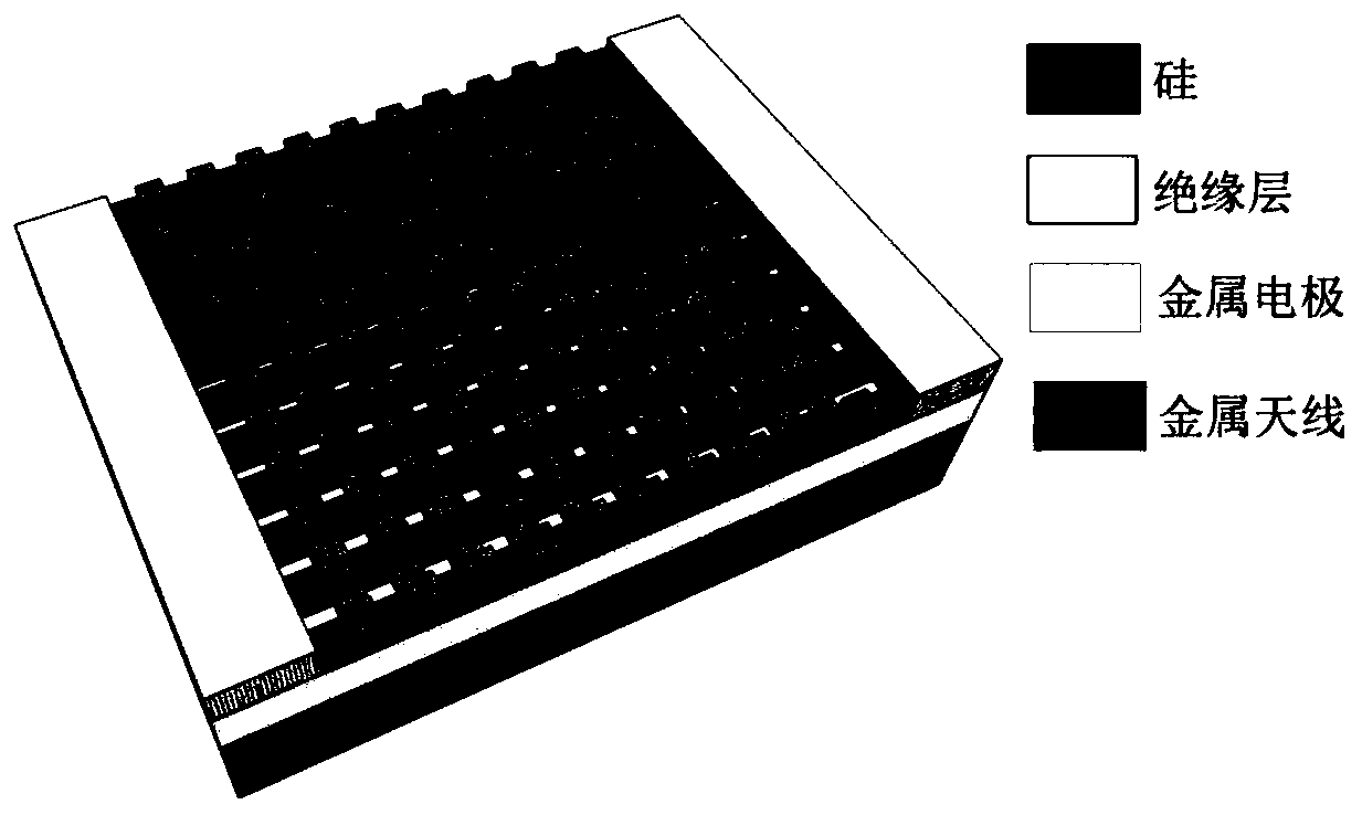
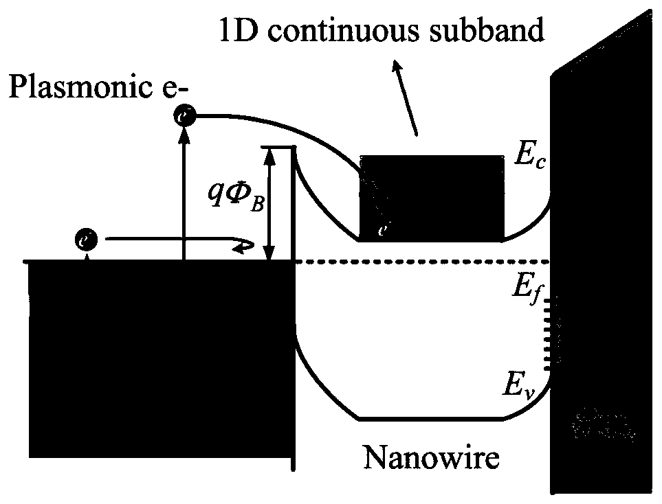
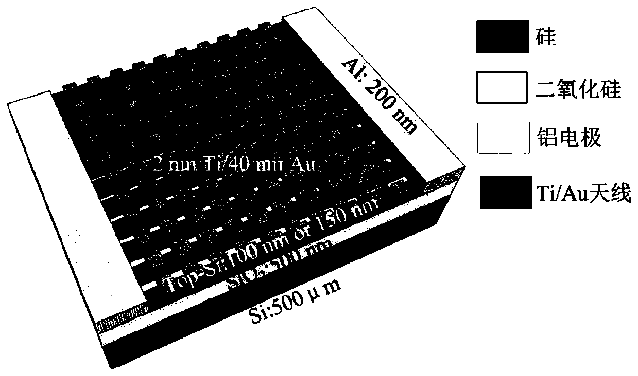
[0059] refer to image 3 As shown, it is a specific embodiment of the present invention, and the whole device structure includes:

[0060] A silicon-on-insulator (SOI) substrate, the thickness of the silicon on the top layer of the substrate is 150 nanometers and 200 nanometers, which is almost intrinsically doped with phosphorus ions, and the doping concentration is 2.8×10 15 cm -3 ; The middle layer is silicon oxide with a thickness of 500 nanometers; the bottom layer is ordinary low-doped n-type silicon with a thickness of 500 microns;

[0061] An array of silicon nanowires distributed in parallel, the silicon nanowires are prepared on the oxide layer and in the top layer of silicon; the nanowire line width is 100 and 150 nanometers, the period is 200 and 400 nanometers, the length is 300 microns, and the overall width of the distribution is is 200 microns;

[0062] A metasurface construction consisting of nanoscale metal antennas. The material is Ti / Au, where the thic...


PUM


Abstract

The invention belongs to the technical field of photoelectric detection, and particularly relates to a multi-channel total-silicon-based infrared thermoelectric detector and a manufacturing method thereof. The detector structure comprises an SOI substrate of which the top layer is n-type doped; a silicon nanowire array which is distributed in parallel and is prepared on the silicon oxide layer ofthe SOI substrate and in the top silicon; a two-dimensional metasurface constructed and integrated in the silicon nanowire array, wherein the metasurface is composed of a nanoscale metal antenna; a top contact electrode covering the two ends of the silicon nanowire array. The detection wave band of the detector is not limited by direct or indirect transition between semiconductor material bands ofa traditional detector, and the whole 1-3 [mu]m wave band can be covered. The problem that an total-silicon material cannot work in the infrared band with the wavelength larger than 1.1 microns is solved, complete compatibility and integration with a silicon-based CCD device or a CMOS reading circuit are achieved, the total-silicon material can be developed into an infrared photoelectric chip ofa multi-channel, high-resolution and a large-area focal plane pixel array, and the total-silicon material has wide application prospects.

Description

technical field [0001] The invention belongs to the technical field of photoelectric detection, and in particular relates to an all-silicon-based infrared photodetector and a manufacturing method thereof. Background technique [0002] The materials currently used in near-infrared photodetection (1-3μm) are almost all dominated by III-V / II-VI materials, such as: InGaAs, HgCdTe, InSb, etc. However, these materials have the following defects: high material cost, high toxicity, causing environmental pollution, extremely complex and unstable material growth and device preparation process, low yield of the prepared device, must work at low temperature, limited by the diameter of the single crystal material ingot It is impossible to achieve a large area (currently the maximum area of ​​GaAs is 6 inches), and it is not compatible with traditional silicon-based CMOS processes and readout circuit chips. On the other hand, the current development trend of infrared focal plane imaging ...

Claims


Application Information

Patent Timeline
Patent Type & Authority Applications(China)
IPC IPC(8): H01L31/0352H01L31/09H01L31/18
CPCH01L31/0352H01L31/035218H01L31/09H01L31/18
Inventor 陈宜方冯波陆冰睿朱静远刘飞飞周磊
Owner FUDAN UNIV
Why Eureka
Try Eureka