Transfer method of semiconductor film layer and preparation method of composite wafer

A transfer method, semiconductor technology, applied in semiconductor/solid-state device manufacturing, electrical components, circuits, etc., can solve problems affecting film quality and heterogeneous integration flexibility, interdiffusion and reverse domain, lattice mismatch, etc. Achieve the effect of promoting industrial application, low cost, and saving manufacturing cost

Active Publication Date: 2019-11-22
BEIJING UNIV OF TECH
View PDF5 Cites 2 Cited by
  • Summary
  • Abstract
  • Description
  • Claims
  • Application Information

AI Technical Summary

Problems solved by technology

In terms of material heterogeneity integration, traditional epitaxial growth methods, such as molecular beam epitaxy, metal organic chemical vapor phase epitaxy, chemical vapor deposition, physical vapor phase epitaxy and magnetron sputtering, etc., have lattice mismatch, crystal form mismatch, Issues such as interdiffusion and reverse domains seriously affect the film quality and the flexibility of heterogeneous integration

Method used


Image

  • Transfer method of semiconductor film layer and preparation method of composite wafer
  • Transfer method of semiconductor film layer and preparation method of composite wafer
  • Transfer method of semiconductor film layer and preparation method of composite wafer

Examples


Embodiment Construction

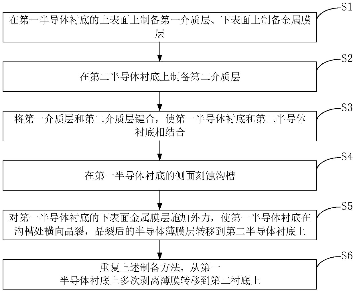
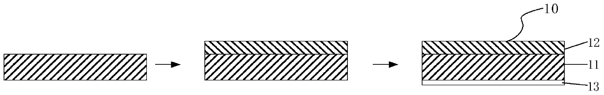
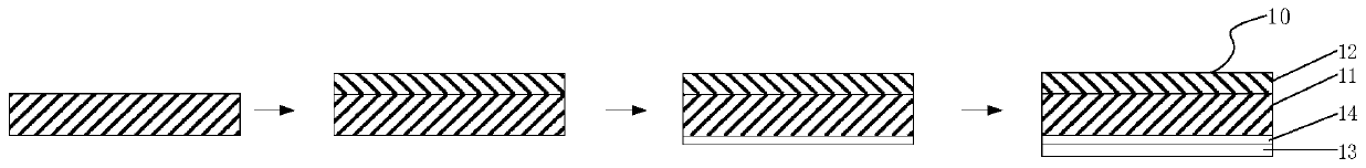
[0056] In order to make the purpose, technical solutions and advantages of the embodiments of the present invention clearer, the technical solutions in the embodiments of the present invention will be clearly and completely described below in conjunction with the drawings in the embodiments of the present invention. Obviously, the described embodiments It is a part of embodiments of the present invention, but not all embodiments. Based on the embodiments of the present invention, all other embodiments obtained by persons of ordinary skill in the art without making creative efforts belong to the protection scope of the present invention.

[0057]In the description of the present invention, it should be noted that the terms "center", "upper", "lower", "left", "right", "vertical", "horizontal", "inner", "outer" etc. The indicated orientation or positional relationship is based on the orientation or positional relationship shown in the drawings, and is only for the convenience of ...


PUM

PropertyMeasurementUnit
thicknessaaaaaaaaaa
thicknessaaaaaaaaaa
thicknessaaaaaaaaaa

Abstract

The invention discloses a transfer method of a semiconductor film layer and a preparation method of a composite wafer. The method comprises the following steps: preparing a first dielectric layer on the upper surface of a semiconductor substrate, and preparing a metal film layer on the lower surface of the semiconductor substrate; preparing a second dielectric layer on the second semiconductor substrate; bonding the first dielectric layer and the second dielectric layer to enable the first semiconductor substrate and the second semiconductor substrate to be combined; etching a groove in the side surface of the first semiconductor substrate; applying external force to the metal film layer on the lower surface of the first semiconductor substrate, so that the first semiconductor substrate issubjected to transverse crystal cracking at the groove, and the semiconductor film layer subjected to crystal cracking is transferred to the second semiconductor substrate. According to the invention, the preparation of the high-quality, large-area and low-cost semiconductor single crystal thin film layer on the XOI substrate can be realized; meanwhile, the method can repeatedly utilize the remaining first semiconductor substrate and separate multiple semiconductor film layers from the first semiconductor substrate for preparing multiple XOIs, so that the industrial manufacturing cost is greatly saved.

Description

technical field [0001] The invention relates to the technical field of semiconductor device integration, in particular to a method for transferring a semiconductor thin film layer and a method for preparing a composite wafer. Background technique [0002] In the future, microelectronics, optoelectronic devices, and intelligent microsystems will continue to develop in the direction of miniaturization, integration, and intelligence, and the required microsystem chip functions will be more complex, diverse, and compatible. This development trend has put forward a huge demand for heterogeneous integration technology, and heterogeneous integration will also open up a new path for the development of microelectronics technology in the post-Moore era; on the basis of maintaining the original device and process size, the development of heterogeneous The integrated integration technology of materials and multiple functional devices can realize the diversification of the functions of a...

Claims


Application Information

Patent Timeline
Patent Type & Authority Applications(China)
IPC IPC(8): H01L21/762H01L21/78
CPCH01L21/76259H01L21/7813
Inventor 代京京王智勇兰天
Owner BEIJING UNIV OF TECH
Why Eureka
Try Eureka