Electroluminescence device based on boron-containing organic compound

An electroluminescent device and organic compound technology, applied in the field of high-efficiency, long-life organic electroluminescent devices, can solve the problems of difficult exciton utilization, high fluorescence radiation efficiency, efficiency roll-off, and large configuration changes. Achieve the effect of reducing the exciton quenching effect and improving efficiency

Active Publication Date: 2019-11-22
JIANGSU SUNERA TECH CO LTD
View PDF5 Cites 29 Cited by
  • Summary
  • Abstract
  • Description
  • Claims
  • Application Information

AI Technical Summary

Problems solved by technology

[0006] Although theoretically TADF materials can achieve 100% exciton utilization, there are actually the following problems: (1) The T1 and S1 states of the designed molecules have strong CT characteristics, and the very small S1-T1 state energy gap, although it can A high T1→S1 state exciton conversion rate is achieved through the TADF process, but at the same time it leads to a low S1 state radiative transition rate. Therefore, it is difficult to achieve both (or simultaneously) high exciton utilization efficiency and high fluorescence radiation effic...

Method used


Image

  • Electroluminescence device based on boron-containing organic compound
  • Electroluminescence device based on boron-containing organic compound
  • Electroluminescence device based on boron-containing organic compound

Examples


Embodiment 1

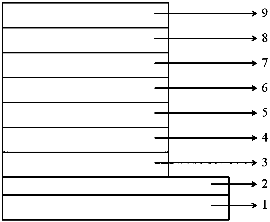
[0110] The structure of the organic electroluminescent device prepared in Example 1 is as follows: figure 1 As shown, the specific preparation process of the device is as follows:

[0111] Clean the ITO anode layer 2 on the transparent glass substrate layer 1, ultrasonically clean it with deionized water, acetone, and ethanol for 30 minutes each, and then treat it in a plasma cleaner for 2 minutes; dry the ITO glass substrate and place it in a vacuum In the cavity, the vacuum degree is less than 1*10 -6 Torr, on the ITO anode layer 2, a mixture of HT1 and P1 with a film thickness of 10 nm is evaporated, the mass ratio of HT1 and P1 is 97:3, and this layer is the hole injection layer 3; then, HT1 with a thickness of 50 nm is evaporated, and the layer As the hole transport layer 4; then vapor-deposit 20nm-thick EB1, which serves as the electron blocking layer 5; further, vapor-deposit a 25nm light-emitting layer 6, wherein the light-emitting layer includes a host material and a...

Embodiment 2~21

[0113] The preparation methods of Examples 2-21 are similar to those of Example 1, and the selection of specific materials is shown in Table 1.


PUM


Abstract

The present invention relates to an electroluminescence device based on a boron-containing organic compound, wherein a main body material comprises a first organic compound and a second organic compound, the difference between a singlet state energy level and a triplet state energy level of the first organic compound is not greater than 0.2 eV, the singlet energy level of the second organic compound is greater than the singlet energy level of the first organic compound by more than 0.1 eV, and the triplet energy level of the second organic compound is greater than the triplet energy level of the first organic compound by more than 0.1 eV; the first organic compound and the second organic compound have the different carrier transport characteristics, wherein an object material is the boron-containing organic compound, the singlet energy level of the object material is lower than that of the first organic compound, and the triplet energy level of the object material is lower than that ofthe first organic compound. An organic light-emitting device prepared by the method has the characteristics of high efficiency and long service life.

Description

technical field [0001] The invention relates to the technical field of semiconductors, in particular to an organic electroluminescent device with high efficiency and long life. Background technique [0002] Organic light emitting diodes (OLEDs) have been actively researched and developed. The simplest basic structure of an organic electroluminescent device consists of a light emitting layer sandwiched between opposing cathode and anode. Organic electroluminescent devices are considered to be the next generation of flat panel display materials and have attracted widespread attention due to their ultra-thin, ultra-light weight, fast response to input signals, and low-voltage DC drive. [0003] It is generally believed that organic electroluminescent devices have the following light-emitting mechanism: when a voltage is applied between electrodes sandwiching a light-emitting layer, electrons injected from the anode and holes injected from the cathode recombine in the light-emi...

Claims


Application Information

Patent Timeline
IPC IPC(8): H01L51/50H01L51/54
CPCH10K85/60H10K50/12H10K2101/30H10K85/626H10K85/633H10K85/6572H10K85/322H10K50/11H10K50/15H10K50/16H10K50/171H10K2101/10H10K2101/40
Inventor 李崇叶中华张兆超
Owner JIANGSU SUNERA TECH CO LTD
Why Eureka
Try Eureka