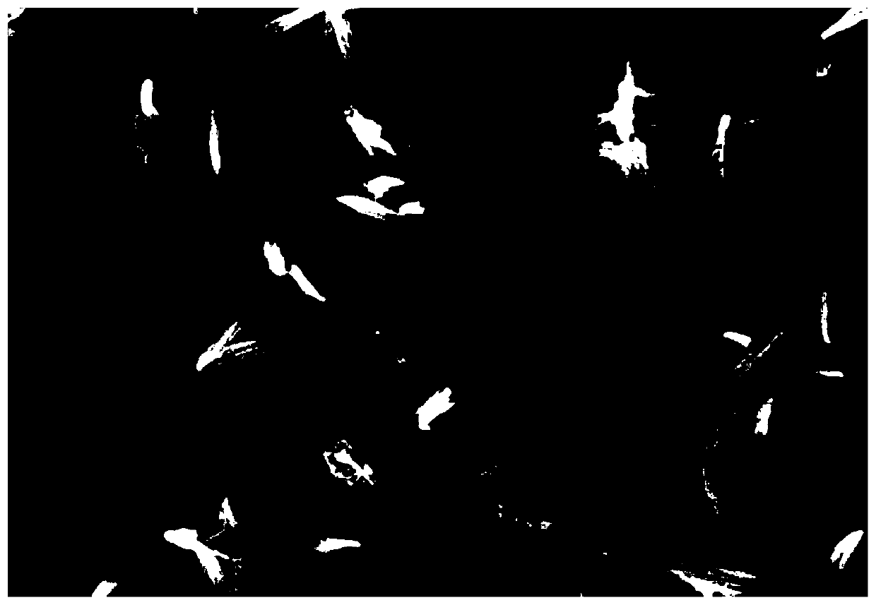
Double-heterostructure surface-enhanced Raman substrate for in-situ detection as well as preparation method and application of double-heterostructure surface-enhanced Raman substrate
A surface-enhanced Raman and double-heterostructure technology, applied in Raman scattering, measurement devices, instruments, etc., can solve the problems of complicated production methods, inability to large-scale preparation, low detection level, etc. Low cost, uniform size effect
- Summary
- Abstract
- Description
- Claims
- Application Information
AI Technical Summary
Problems solved by technology
Method used
Image
Examples
Embodiment 1
[0040] Cut the polyester resin flexible film into square pieces of 1 square centimeter, put them in the cleaning solution for cleaning for 1 to 10 minutes, and blow dry with nitrogen gas.
[0041] Put the above-mentioned film into a plasma cleaner for cleaning for 2 to 3 minutes to increase its surface hydrophilicity.
[0042] Put the cleaned polyester resin film into a magnetron sputtering apparatus, set the power to 100 watts, and the pressure to 10-6 Pa, and sputter the copper oxide seed crystal layer with a sputtering thickness of about 60 nanometers.
[0043] The above-mentioned film was placed on the anode end of the electrochemical cell of the two-electrode system, the cathode end was selected as an aluminum electrode, the electrolyte was sodium hypochlorite solution, the voltage was 5 volts, the current was 10 mA, and copper oxide nanowires were electrochemically deposited for 800 seconds.
[0044] The polyester resin film grown with copper peroxide nanowires is cleane...
Embodiment 2
[0051] Cut the polyester resin flexible film into square pieces of 1 square centimeter, put them in the cleaning solution for cleaning for 1 to 10 minutes, and blow dry with nitrogen gas.
[0052] Put the above-mentioned film into a plasma cleaner for cleaning for 2 to 3 minutes to increase its surface hydrophilicity.
[0053] Put the cleaned polyester resin film into a magnetron sputtering apparatus with a power setting of 100 watts and a pressure of 10-6 Pa to sputter a copper oxide seed layer with a sputtering thickness of about 80 nanometers.
[0054]The above-mentioned film was placed on the anode end of the electrochemical cell of the two-electrode system, the cathode end was selected as an aluminum electrode, the electrolyte was sodium hypochlorite solution, the voltage was 6 volts, the current was 11 mA, and copper oxide nanowires were electrochemically deposited for 850 seconds.
[0055] The polyester resin film grown with copper peroxide nanowires is cleaned in a pla...
PUM
| Property | Measurement | Unit |
|---|---|---|
| thickness | aaaaa | aaaaa |
Abstract
Description
Claims
Application Information
 - R&D
- Intellectual Property
- Life Sciences
- Materials
- Tech Scout
- Unparalleled Data Quality
- Higher Quality Content
- 60% Fewer Hallucinations
Browse by: Latest US Patents, China's latest patents, Technical Efficacy Thesaurus, Application Domain, Technology Topic, Popular Technical Reports.
© 2025 PatSnap. All rights reserved.Legal|Privacy policy|Modern Slavery Act Transparency Statement|Sitemap|About US| Contact US: help@patsnap.com


