Semiconductor thin film field effect transistor of a kind of unstable two-dimensional material and preparation method thereof

A technology of thin film field effect and two-dimensional materials, which is applied in semiconductor/solid-state device manufacturing, semiconductor devices, transistors, etc. The effect of small hysteresis and short exposure time

Active Publication Date: 2021-01-15
SHANDONG UNIV
View PDF5 Cites 0 Cited by
  • Summary
  • Abstract
  • Description
  • Claims
  • Application Information

AI Technical Summary

Problems solved by technology

However, the disadvantage of the mechanical exfoliation method is that the thickness of the nanosheets obtained by the exfoliation and its distribution on the substrate are very random, the position cannot be controlled, and the output of the device is small.
However, this method has many disadvantages corresponding to the mechanical exfoliation method: the two-dimensional material film transferred by the mechanical exfoliation method is random, and the thickness, size, and position cannot be precisely controlled
However, these methods have different disadvantages: (1) PMMA is not compatible with the photolithography process and will dissolve when encountering organic solvents
Due to the need for positive sample spin-coating, the contact between the electrode and the probe will also be affected during the test
(2) Using BN sheets to cover, the process is difficult, the alignment is difficult, and the success rate is low. It is usually completed in the glove box, and the efficiency is relatively low.
(3) Oxidize the surface of InSe to make the surface of InSe into InO x , the oxidation process has low controllability and cannot be applied to thin-layer InSe materials
(4) The method of evaporating In has low controllability, and the effective channel length of the device will be reduced which is difficult to measure, which will cause errors in the extraction of intrinsic parameters of the device and material
It is also not suitable for the production of optoelectronic devices

Method used


Image

  • Semiconductor thin film field effect transistor of a kind of unstable two-dimensional material and preparation method thereof
  • Semiconductor thin film field effect transistor of a kind of unstable two-dimensional material and preparation method thereof
  • Semiconductor thin film field effect transistor of a kind of unstable two-dimensional material and preparation method thereof

Examples


Embodiment 1

[0059] A semiconductor thin film field effect transistor of an unstable two-dimensional material, which comprises a silicon wafer substrate, an unstable two-dimensional material, an aluminum oxide film, a source electrode and a drain electrode sequentially from bottom to top.

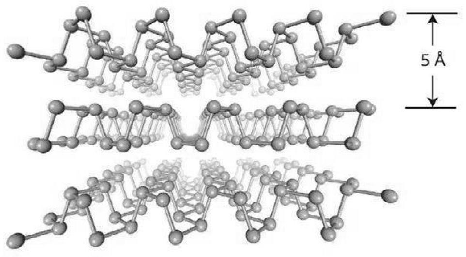
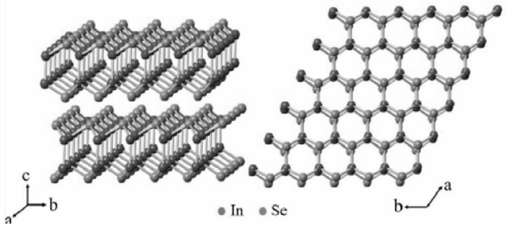
[0060] Unstable two-dimensional materials are indium selenide (InSe), black phosphorus, transition metal sulfides, or III-VI compounds. The thickness of the unstable 2D material is 20-80nm. The aluminum oxide thin film has a thickness of 20 nm.

Embodiment 2

[0062] According to the semiconductor thin film field effect transistor of an unstable two-dimensional material described in Embodiment 1, the difference lies in that the thickness of the aluminum oxide film is 40 nm.

Embodiment 3

[0064] According to the semiconductor thin film field effect transistor of an unstable two-dimensional material described in Embodiment 1, the difference lies in that the thickness of the aluminum oxide film is 30 nm. The 30nm alumina can play a better isolation effect, so that the process solvent and air have less influence on the semiconductor material, and at the same time, the photoresist will not be etched too much due to the relatively small etching selection during the rear etching. This results in difficulty in electrode stripping.


PUM

PropertyMeasurementUnit
thicknessaaaaaaaaaa
thicknessaaaaaaaaaa
thicknessaaaaaaaaaa

Abstract

The invention relates to a semiconductor film field effect transistor made of an unstable two-dimensional material and a preparation method thereof. The field effect transistor sequentially comprisesa silicon wafer substrate, the unstable two-dimensional material, an aluminum oxide film, a source electrode and a drain electrode from bottom to top. According to the method, the unstable two-dimensional material in the air and the solvent can be obtained through a simple method, and a small-size electronic device can be obtained through the micro-nano machining technology, moreover, the field effect mobility can reach the level of the hard mask process, and the yield is higher. For an InSe film, the highest field effect mobility exceeds 550 cm<2> / Vs. A device channel is protected by a packaging buffer layer at the same time, and the performance is not reduced in the air environment as long as 60 days. The aluminum oxide packaging buffer layer is stable and transparent, and can be appliedto further manufacturing of photoelectric micro-nano devices, and the electric hysteresis phenomenon is small (less than 1V).

Description

technical field [0001] The invention relates to a semiconductor thin film field effect transistor of an unstable two-dimensional material and a preparation method thereof, belonging to the technical field of semiconductor technology. Background technique [0002] Since the discovery of graphene, the research on two-dimensional layered materials has set off a wave of upsurge. So far, a large number of high-quality two-dimensional layered semiconductor materials have been developed and studied, mainly including three types: transition metal sulfides, black phosphorus, and III-VI selenides. [0003] Among many two-dimensional materials, black phosphorus and indium selenide with high theoretical mobility have the disadvantage of unstable properties in air and solvent environments. Due to the lone pair of electrons on the phosphorus atom of the fifth main group, black phosphorus will rapidly degrade when it encounters water or oxygen to form phosphoric acid. The high mobility o...

Claims


Application Information

Patent Timeline
Patent Type & Authority Patents(China)
IPC IPC(8): H01L29/786H01L21/336H01L21/263
CPCH01L21/2633H01L29/66772H01L29/78684H01L29/78696
Inventor 王一鸣宋爱民梁广大辛倩
Owner SHANDONG UNIV
Why Eureka
Try Eureka