

Manufacturing process of embedded radar antenna PCB
A technology of radar antenna and manufacturing process, which is suitable for antennas on movable objects, printed circuit manufacturing, and structural forms of radiating elements, etc. It can solve the problem of large line width and line gap tolerance, rough plating on the board surface, and affecting radar performance, etc. problem, to achieve the effect of zero line width and gap tolerance, precise graphics, and avoid dents and copper bumps
- Summary
- Abstract
- Description
- Claims
- Application Information
AI Technical Summary
Problems solved by technology
Method used
Image

Examples
Embodiment 1
[0070] All the radar antenna circuit boards made by non-etching process and embedded in or embedded on the PCB substrate by lamination method belong to the scope of protection of this patent. Radar sensor antenna circuit board (radar sensors include microwave, millimeter wave, ultrasonic, laser, infrared, camera).
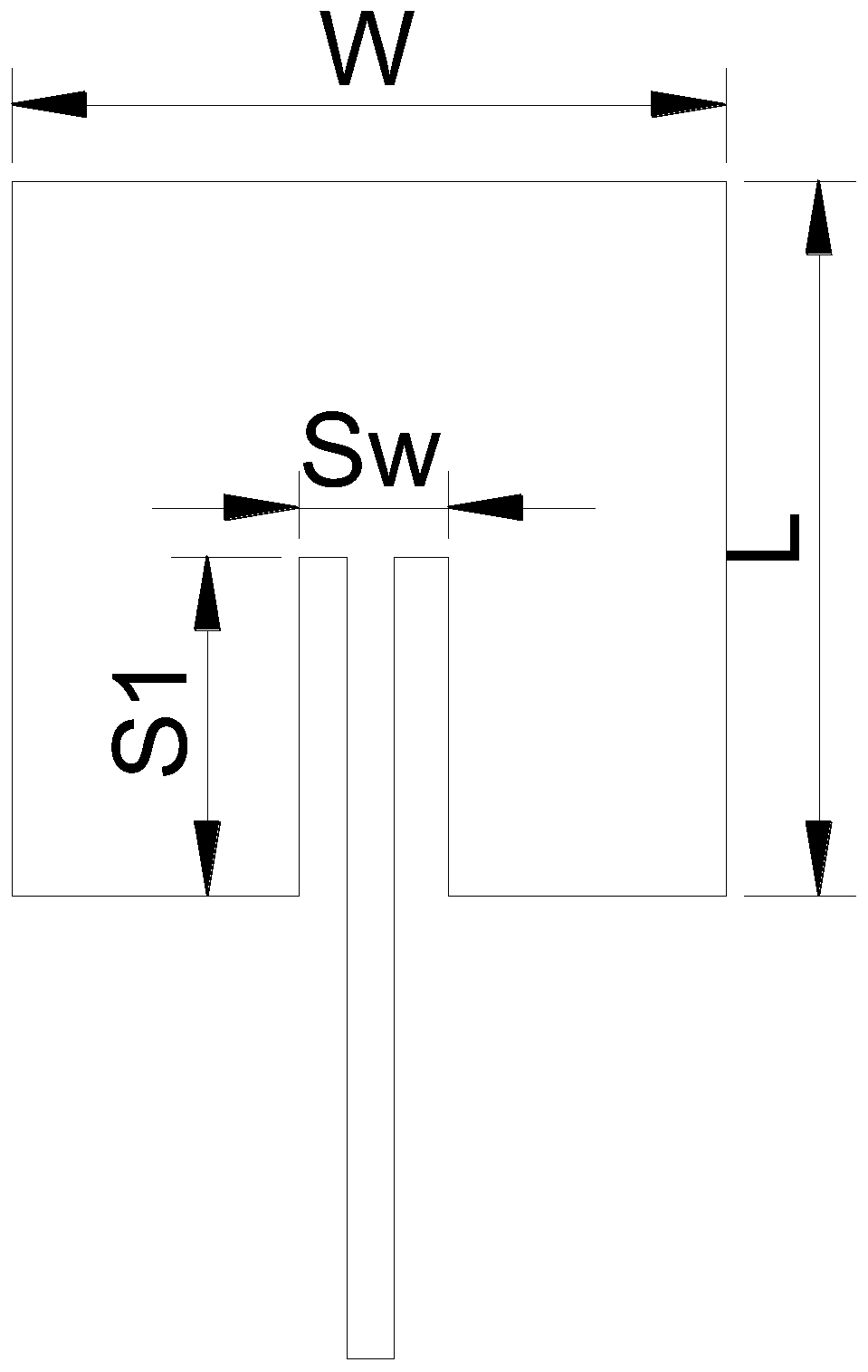
[0071] Since the microstrip feeder and the microstrip copper array element are coplanar, they can be etched together during processing, so it is very convenient to use the microstrip line to feed the microstrip array unit. The feed structure uses a microstrip line to feed the center of the broadside, and the feed line and the copper pad are on the same plane, such as figure 1 As shown, a slot with a width of Sw is opened on the copper sheet, and the feeder is inserted into the middle of the copper pad for electricity. Sl is the distance between the feed point and the edge of the copper PAD, and Sw is the slot width. By adjusting the size of Sl and Sw, the input im...
Embodiment 2
[0073] In order to achieve the best antenna performance, the feeder line width of the microstrip antenna is generally designed to be 0.124mm and the distance from the feeder to the slot edge is designed to be 0.10mm. Then, in order to take into account the 25um copper thickness in the hole during PCB processing, the general surface copper thickness must be at least 38um. .
[0074] Because the traditional DES and SES etching are affected by etching temperature, concentration, PH value, etching factor and pool effect, it is difficult to accurately etch the line width and line gap pattern for a line width of 0.124mm and a line gap of 0.1mm, which will affect the performance of the Radar sensor .
[0075] For this reason, this patent researches a new antenna circuit board manufacturing process technology, and adopts the method of non-etching and embedding lines to manufacture millimeter-wave Radar antennas, thereby avoiding graphic variation due to etching factors, uneven line wi...
PUM
 Abstract
Description
Claims
Application Information