Method and product of coating nanocrystalline thin film based on plasma atomic layer deposition

A technology of atomic layer deposition and plasma, which is applied in the direction of liquid-coating devices, coatings, gaseous chemical plating, etc., can solve the problem of loss of luminous performance and achieve the effect of facilitating mass production

Active Publication Date: 2021-01-19
HUAZHONG UNIV OF SCI & TECH
View PDF4 Cites 0 Cited by
  • Summary
  • Abstract
  • Description
  • Claims
  • Application Information

AI Technical Summary

Problems solved by technology

[0005] Aiming at the above defects or improvement needs of the prior art, the present invention provides a method and product based on plasma atomic layer deposition coating nanocrystalline film, by adopting plasma-enhanced atomic layer deposition method to deposit and oxidize the surface of nanocrystalline film Silicon cladding layer, in this way, can not only effectively solve the problem that nanocrystals are susceptible to water and oxygen erosion, causing them to lose their luminescent properties, but also has the advantages of easy manipulation, strong adaptability, low cost and suitable for mass production.

Method used


Image

  • Method and product of coating nanocrystalline thin film based on plasma atomic layer deposition

Examples


preparation example Construction

[0027] A method for coating a nanocrystalline film based on plasma atomic layer deposition, the preparation method mainly includes the following steps:

[0028] Step 1. Preparation of nanocrystalline colloid

[0029] Mix oleylamine, oleic acid, and lead bromide according to the ratio of mass fraction of 12-18:7-10:1-4, and heat to 150°C-180°C under an inert atmosphere until a completely dissolved precursor is formed; Immediately inject a certain proportion of cesium stearate-octadecene mixed solution into the precursor, the mass ratio of cesium stearate to octadecene in the mixed solution is 1~3:10~15, and the reaction is 5s~ After 10s, place the whole in an ice-water mixture to cool and stop the reaction; then, centrifuge and purify the reaction product quantum dot colloid and add n-hexane solution. The mass ratio of quantum dot colloid to n-hexane solution is 0.5-1:10-15. Formation of nanocrystalline colloids.

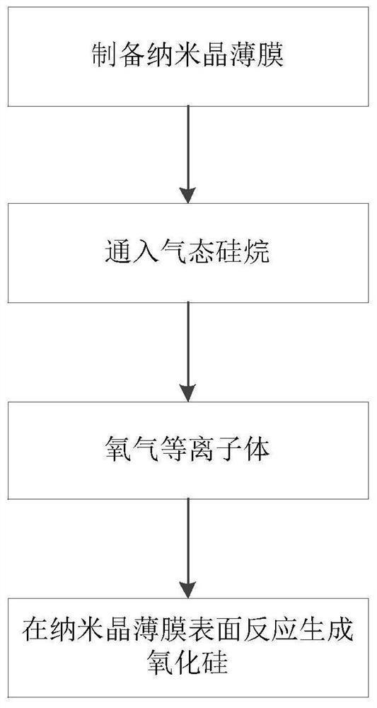
[0030] Step 2, preparing a nanocrystalline thin film.

[003...

Embodiment 1

[0041] (a1) Mix oleylamine solution, oleic acid solution, and lead bromide powder to form a mixed solution, and heat to 150° C. under an inert atmosphere to fully dissolve the mixed solution to obtain a precursor solution. In the precursor solution, oleylamine, oil The ratio of acid and lead bromide mass fraction is 12:7:1;

[0042] (a2) Add cesium stearate-octadecene mixed solution in the precursor solution, react for 5s, obtain the quantum dot colloid with this, centrifugally purify the quantum dot colloid, then add n-hexane solution, form nanocrystalline colloid with this, Wherein, the cesium stearate-octadecene mixed solution is a mixed solution formed by mixing cesium stearate and octadecene according to a mass ratio of 1:10, and the mass ratio of quantum dot colloid and n-hexane solution is 0.5:10;

[0043] (a3) The nanocrystalline colloid obtained in step (a2) is spin-coated on the carrier, and the desired nanocrystalline film is obtained after curing, wherein the rotat...

Embodiment 2

[0048] (a1) Mix oleylamine solution, oleic acid solution, and lead bromide powder to form a mixed solution, and heat to 180° C. under an inert atmosphere to fully dissolve the mixed solution to obtain a precursor solution. In the precursor solution, oleylamine, oil The ratio of acid and lead bromide mass fraction is 18:10:4;

[0049] (a2) Add cesium stearate-octadecene mixed solution to the precursor solution, and react for 10s to obtain the quantum dot colloid, then centrifugally purify the quantum dot colloid, and then add n-hexane solution to form nanocrystalline colloid, Wherein, the cesium stearate-octadecene mixed solution is a mixed solution formed by mixing cesium stearate and octadecene according to a mass ratio of 3:15, and the mass ratio of quantum dot colloid and n-hexane solution is 1:15;

[0050] (a3) The nanocrystalline colloid obtained in step (a2) is spin-coated on the carrier, and the desired nanocrystalline film is obtained after curing, wherein the rotation...


PUM

PropertyMeasurementUnit
thicknessaaaaaaaaaa
particle diameteraaaaaaaaaa

Abstract

The invention belongs to the field of preparation of nanocrystalline films, and particularly discloses a method for coating a nanocrystalline film based on plasma atomic layer deposition and a product. The method comprises the following steps that (a) the nanocrystalline film is prepared, and the obtained nanocrystalline film is put in a reaction cavity of an atomic layer deposition device and heated; (b) gaseous silane is introduced into the reaction cavity to react with the nanocrystalline film, and carrier gas is continuously introduced in the reaction process to keep the gas pressure in the reaction cavity constant; (c) oxygen plasma is introduced into the reaction cavity, carrier gas is continuously introduced in the reaction process to keep the gas pressure in the reaction cavity constant, silicon oxide is generated, and the surface of the nanocrystalline film is coated with silicon oxide; and (d) the steps (b)-(c) are repeated until the thickness of silicon oxide reaches a preset thickness value. By means of the method, the problem that nanocrystalline is prone to being eroded by water and oxygen and accordingly the luminescence performance of the nanocrystalline is lost issolved. The method has the advantages of being convenient to control, high in adaptability, low in cost, suitable for mass production and the like.

Description

technical field [0001] The invention belongs to the field of preparation of nanocrystalline thin films, and more specifically relates to a method and product for coating nanocrystalline thin films based on plasma atomic layer deposition. Background technique [0002] Nanocrystals, also known as quantum dots, are nanoparticles composed of II-VI or III-V elements. Its particle size is generally between 1 and 10 nm. Since electrons and holes are quantum-confined, the continuous energy band structure becomes a discrete energy level structure with molecular characteristics, and can emit fluorescence after being excited. The emission spectrum of quantum dots can be controlled by changing the size of quantum dots, which has the effects of adjustable band gap, wide excitation spectrum and narrow emission spectrum, and has a wide range of applications in solar cells, light-emitting devices, optical biomarkers and other fields prospect. [0003] Although quantum dots have excellent ...

Claims


Application Information

Patent Timeline
Patent Type & Authority Patents(China)
IPC IPC(8): C23C16/455C23C16/40B05D1/00B05D7/04B05D7/24
CPCB05D1/005B05D7/04B05D7/24C23C16/402C23C16/4554
Inventor 陈蓉井尧曹坤周彬泽姜晨晨耿士才刘梦佳
Owner HUAZHONG UNIV OF SCI & TECH
Why Eureka
Try Eureka