GaN-based field effect transistor and preparation method thereof

A GaN-based field and transistor technology, which is applied in semiconductor/solid-state device manufacturing, semiconductor devices, electrical components, etc., can solve the problems of two-dimensional electron gas depletion, the influence of two-dimensional electron gas concentration, and the reduction of device characteristics.

Inactive Publication Date: 2020-01-14
SOUTH UNIVERSITY OF SCIENCE AND TECHNOLOGY OF CHINA
View PDF7 Cites 6 Cited by
  • Summary
  • Abstract
  • Description
  • Claims
  • Application Information

AI Technical Summary

Problems solved by technology

Over-etching of the barrier layer 50 will damage the barrier layer, and will also affect the two-dimensional electron gas concentration in the channel layer, reducing the device characteristics; if the etching stops before reaching the barrier layer 50, the barrier layer will be reduced. The remaining part of the p-type gate layer material on the top of layer 50 leads to the depletion of the two-dimensional electron gas in the channel layer, reducing the current output capability of the device.
The residue of the p-type gate layer material will also cause leakage between the gate and the drain; although the etching conditions can be continuously improved, when the etching reaches the surface of the barrier layer, it will cause damage to this layer of material, making the device deteriorating static and dynamic operating characteristics of

Method used


Image

  • GaN-based field effect transistor and preparation method thereof
  • GaN-based field effect transistor and preparation method thereof
  • GaN-based field effect transistor and preparation method thereof

Examples


Embodiment Construction

[0050] The present invention will be further described in detail below in conjunction with the accompanying drawings and embodiments. It should be understood that the specific embodiments described here are only used to explain the present invention, but not to limit the present invention. In addition, it should be noted that, for the convenience of description, only some structures related to the present invention are shown in the drawings but not all structures.

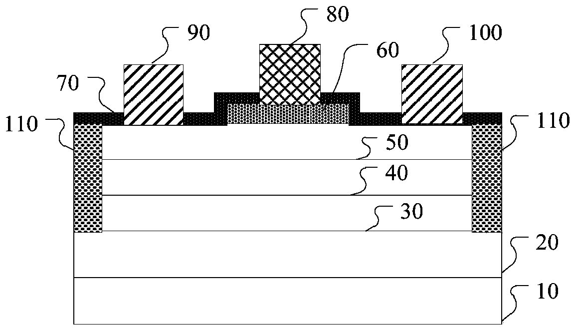
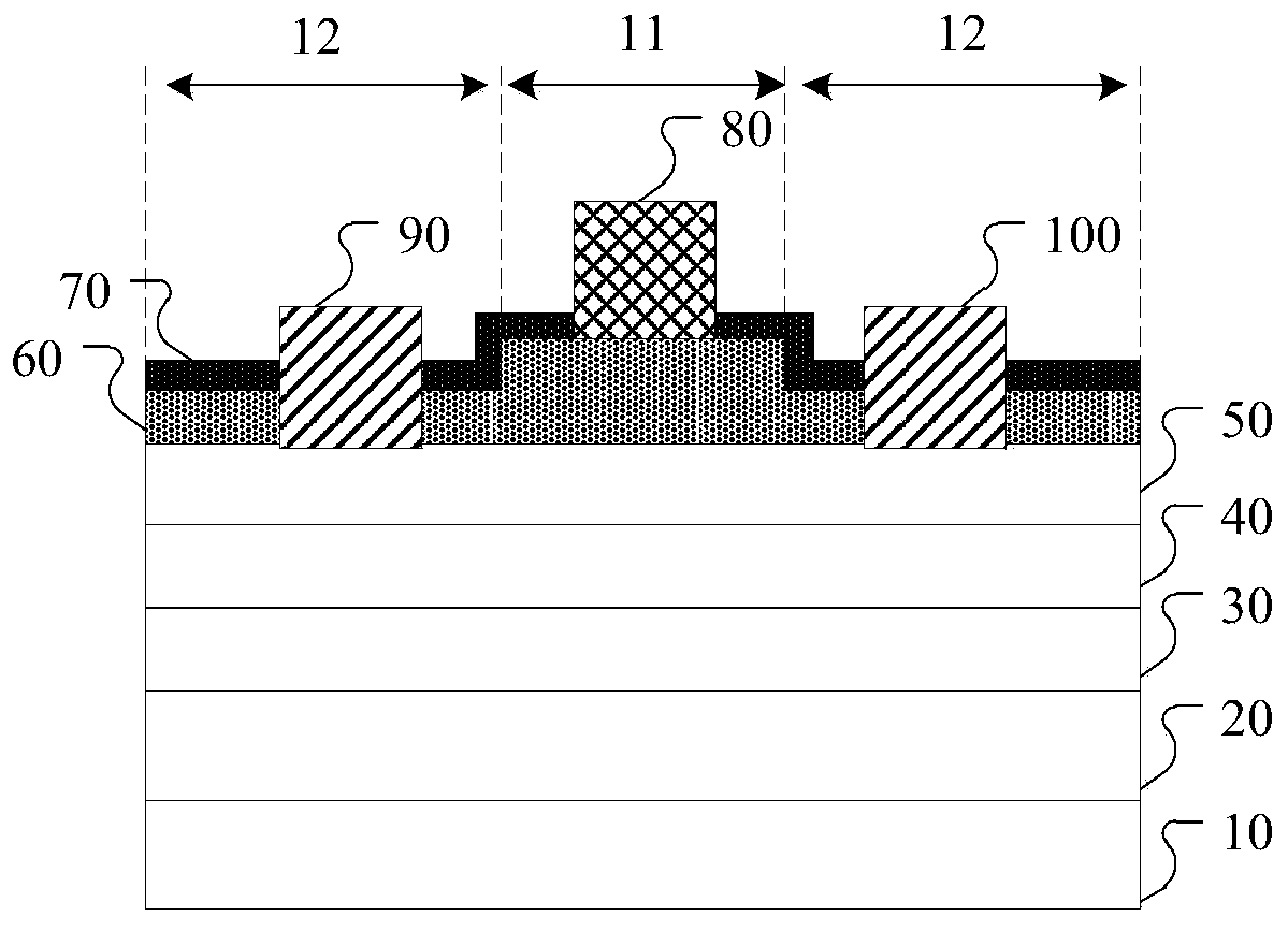
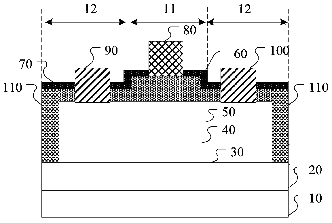
[0051] An embodiment of the present invention provides a GaN-based field effect transistor, referring to figure 1 , figure 1 It is a schematic structural diagram of a GaN-based field effect transistor provided in Embodiment 1 of the present invention, including:

[0052] Stacked substrate 10, buffer layer 20, back barrier layer 30, channel layer 40, barrier layer 50, p-type gate layer 60 and passivation layer 70;

[0053] Gate 80 in contact with p-type gate layer 60, and source 90 and drain 100 penetrating throu...


PUM

PropertyMeasurementUnit
thicknessaaaaaaaaaa
thicknessaaaaaaaaaa
thicknessaaaaaaaaaa

Abstract

The embodiment of the invention discloses a GaN-based field effect transistor and a preparation method thereof. The GaN-based field effect transistor structurally comprises a substrate, a buffer layer, a back barrier layer, a channel layer, a barrier layer, a p-type gate layer and a passivation layer; a gate electrode which is in contact with the p-type gate layer; a source electrode and a drain electrode which are in contact with the barrier layer, wherein the gate electrode is located in the first region, the source electrode and the drain electrode are located in the second region, and thep-type dopant of the p-type gate layer in the film layer of the second region is not activated. According to the technical scheme, the gate etching process is remarkably improved, the problem that p-type materials must be completely removed in a traditional process is solved, the error-tolerant rate of etching is lower, the method is suitable for mass production, the width of a process window of gate etching is increased through the technical method, the method is not limited by the precision of the etching process, and gate electrode etching is high in controllability and good in repeatability.

Description

technical field [0001] Embodiments of the present invention relate to the technical field of semiconductor devices, in particular to a GaN-based field effect transistor and a manufacturing method thereof. Background technique [0002] Conventional gallium nitride (GaN)-based heterojunction transistors are generally depleted normally-on structures (D-Mode), and in circuit design, people prefer to use enhanced normally-off devices (E-Mode), Because the circuit using this type of device has high power-down safety and simple protection circuit. There are many conventional ways to realize enhancement-mode GaN-based heterojunction transistors, such as trench gate structure, fluorine ion implantation at the bottom of gate, metal insulating layer semiconductor gate structure combined with trench gate, p-type gate structure, stacked structure, etc. Among them, the p-type gate structure is a relatively common E-Mode structure, and its structure is simple and easy to process. The con...

Claims


Application Information

Patent Timeline
Patent Type & Authority Applications(China)
IPC IPC(8): H01L29/778H01L21/335
CPCH01L29/7786H01L29/66462
Inventor 于洪宇曾凡明汪青林新鹏周智辉
Owner SOUTH UNIVERSITY OF SCIENCE AND TECHNOLOGY OF CHINA
Why Eureka
Try Eureka