
A kind of high-brightness light-emitting diode based on Aln/PSS composite substrate and preparation method thereof

A technology of light-emitting diodes and composite substrates, applied in semiconductor devices, electrical components, circuits, etc., can solve problems such as high brightness and insufficient brightness, and achieve the effects of high brightness, improved current expansion, and improved luminous efficiency

Active Publication Date: 2020-09-11
DONGGUAN UNIV OF TECH
View PDF1 Cites 0 Cited by
  • Summary
  • Abstract
  • Description
  • Claims
  • Application Information

AI Technical Summary

Problems solved by technology

[0005] In order to overcome the defect of insufficient brightness described in the above-mentioned prior art, the present invention provides a high-brightness light-emitting diode based on an AlN / PSS composite substrate, and the light-emitting diode provided has high luminous efficiency and high brightness

Method used


Image

  • A kind of high-brightness light-emitting diode based on Aln/PSS composite substrate and preparation method thereof
  • A kind of high-brightness light-emitting diode based on Aln/PSS composite substrate and preparation method thereof

Examples


Embodiment 1

[0037] A high-brightness light-emitting diode based on AlN / PSS composite substrate, such as figure 1As shown, it includes an AlN / PSS composite substrate 101, a u-type GaN merged layer 102, an n-type GaN layer 103, a low-temperature GaN V-pits layer 104, an active region 105, and an electron blocking layer 106 stacked sequentially from bottom to top. , a high temperature p-type GaN layer 107 and a contact layer 108 .

[0038] The high-brightness light-emitting diode is prepared through the following preparation steps:

[0039] S1. In a mixed atmosphere of hydrogen and ammonia, at a temperature of 950-1000° C., perform surface activation treatment on the AlN / PSS composite substrate; the reaction chamber pressure is 100 torr, and the treatment is performed for 5-10 minutes.

[0040] S2. Introducing ammonia gas, growing a u-type GaN merged layer on the AlN / PSS composite substrate (101);

[0041] The u-type GaN merged layer includes the first u-type GaN layer, the second u-type G...

Embodiment 2

[0054] This embodiment is the second embodiment of the high-brightness light-emitting diode based on the AlN / PSS composite substrate of the present invention, such as figure 1 As shown, it includes an AlN / PSS composite substrate 101, a u-type GaN merged layer 102, an n-type GaN layer 103, a low-temperature GaN V-pits layer 104, an active region 105, and an electron blocking layer 106 stacked sequentially from bottom to top. , a high temperature p-type GaN layer 107 and a contact layer 108 .

[0055] The high-brightness light-emitting diode is prepared through the following preparation steps:

[0056] S1. In a mixed atmosphere of hydrogen and ammonia, at a temperature of 950-1000° C., perform surface activation treatment on the AlN / PSS composite substrate; the reaction chamber pressure is 100 torr, and the treatment is performed for 5-10 minutes.

[0057] S2. Introducing ammonia gas, growing a u-type GaN merged layer on the AlN / PSS composite substrate (101);

[0058] The u-ty...


PUM

PropertyMeasurementUnit
thicknessaaaaaaaaaa
thicknessaaaaaaaaaa
thicknessaaaaaaaaaa

Abstract

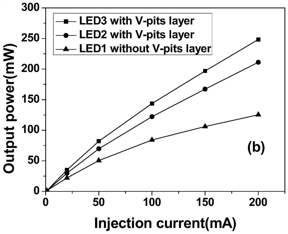
The invention discloses a high-brightness light-emitting diode based on an AIN / PSS composite substrate and a preparation method of the high-brightness light-emitting diode. The high-brightness light-emitting diode comprises the AlN / PSS composite substrate, a u-type GaN merging layer, an n-type GaN layer, a low-temperature GaN V-pits layer, an active region, an electron blocking layer, a high-temperature p-type GaN layer and a contact layer which are sequentially stacked from bottom to top. The high-brightness light-emitting diode provided by the invention comprises the u-GaN merging layer of anovel structure, the V-pits layer and the active region; and therefore, the crystal quality of an epitaxial layer can be effectively improved, the stress of the active region can be effectively relieved, current expansion in a horizontal direction can be improved, the light-emitting efficiency of the light-emitting diode can be improved, and the brightness of the prepared light-emitting diode ishigh.

Description

technical field [0001] The invention relates to the technical field of light-emitting diodes, and more specifically, to a high-brightness light-emitting diode based on an AlN / PSS composite substrate and a preparation method thereof. Background technique [0002] The existing gallium nitride-based light-emitting diodes are mainly prepared on the polar plane: <0001> plane sapphire. Sapphire and gallium nitride belong to the hexagonal crystal, and GaN thin films are usually grown on heterogeneous sapphire. Due to the huge lattice mismatch and thermal mismatch between the two, the threading dislocation (TD) density generated during the epitaxial growth of GaN film is as high as 10 8 ~10 10 / cm 2 . When these TDs extend approximately vertically, they are accompanied by the formation of V-shaped defects with 6 sides of an inverted hexagonal pyramid and {10-11} planes, which are commonly called V-shaped pits (V-pits). [0003] As a typical feature of InGaN / GaN-based LED d...

Claims


Application Information

Patent Timeline
Patent Type & Authority Patents(China)
IPC IPC(8): H01L33/06H01L33/12H01L33/14H01L33/22H01L33/32H01L33/00
CPCH01L33/0066H01L33/0075H01L33/06H01L33/12H01L33/145H01L33/22H01L33/325
Inventor 贾传宇胡西多
Owner DONGGUAN UNIV OF TECH
Learn More