Ultraviolet nanosecond laser direct-writing micro-fluidic chip preparation system and method

A microfluidic chip, laser direct writing technology, applied in laser welding equipment, chemical instruments and methods, manufacturing tools, etc., can solve problems such as lack of flexibility in processing methods, achieve simple and controllable operation and debugging, and low system environment requirements , The effect of low processing cost

Active Publication Date: 2020-02-04
广州市凯佳光学科技有限公司
View PDF8 Cites 2 Cited by
  • Summary
  • Abstract
  • Description
  • Claims
  • Application Information

AI Technical Summary

Problems solved by technology

This technology still has technical barriers to the application of ultraviolet laser and laser cutting head processing, and the processing method lacks flexibility for processing large-scale structures

Method used


Image

  • Ultraviolet nanosecond laser direct-writing micro-fluidic chip preparation system and method
  • Ultraviolet nanosecond laser direct-writing micro-fluidic chip preparation system and method
  • Ultraviolet nanosecond laser direct-writing micro-fluidic chip preparation system and method

Examples


Embodiment Construction

[0046] In order to make the technical means, creative features, goals and effects of the present invention easy to understand, the present invention will be further elaborated below in conjunction with specific illustrations. In the description of the present invention, it should be noted that unless otherwise specified and Limitation, the terms "installation", "connection" and "connection" should be understood in a broad sense, for example, it can be a fixed connection, it can also be a detachable connection, or an integral connection can be a mechanical connection or an electrical connection; it can be It can be directly connected, or indirectly connected through an intermediary, and can be connected internally between two components.

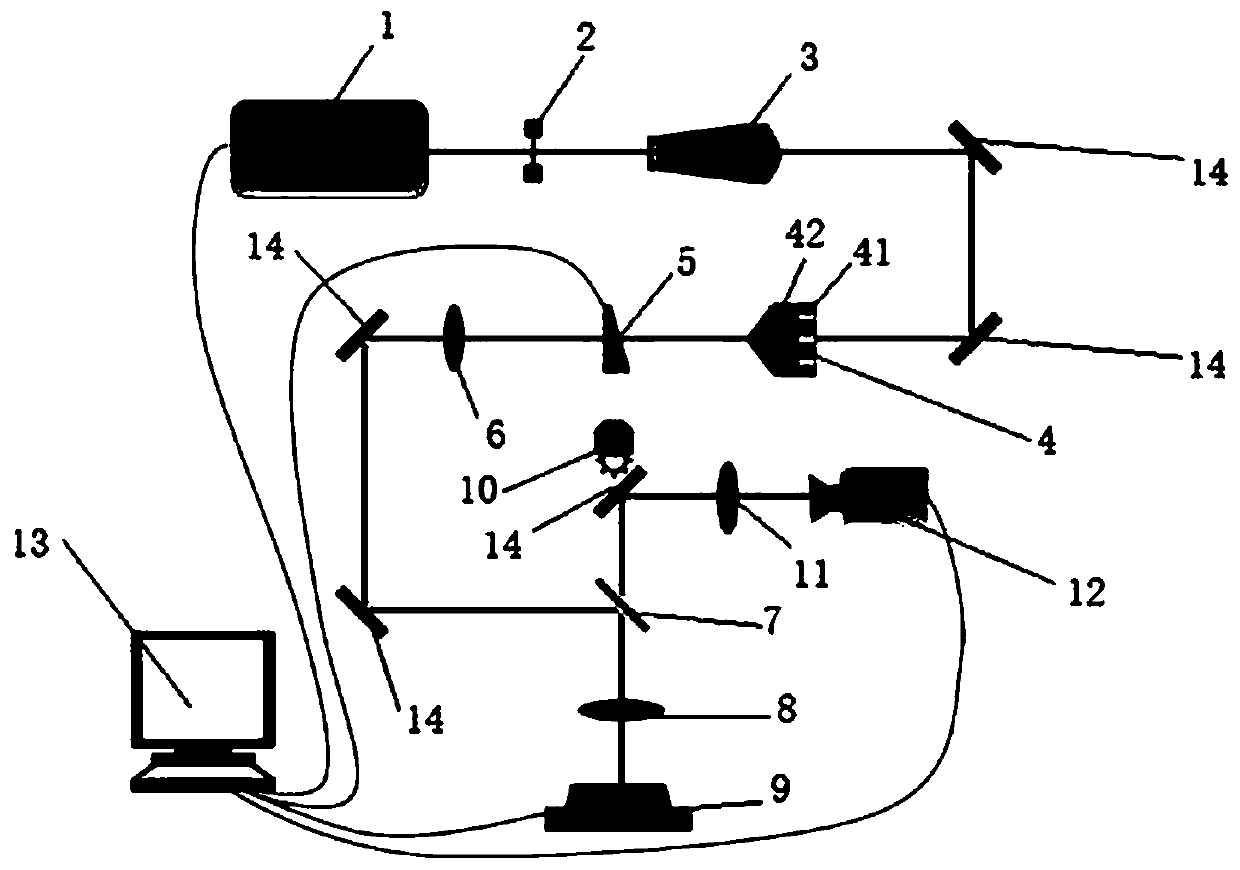
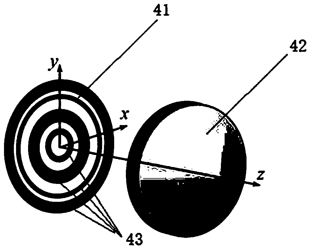
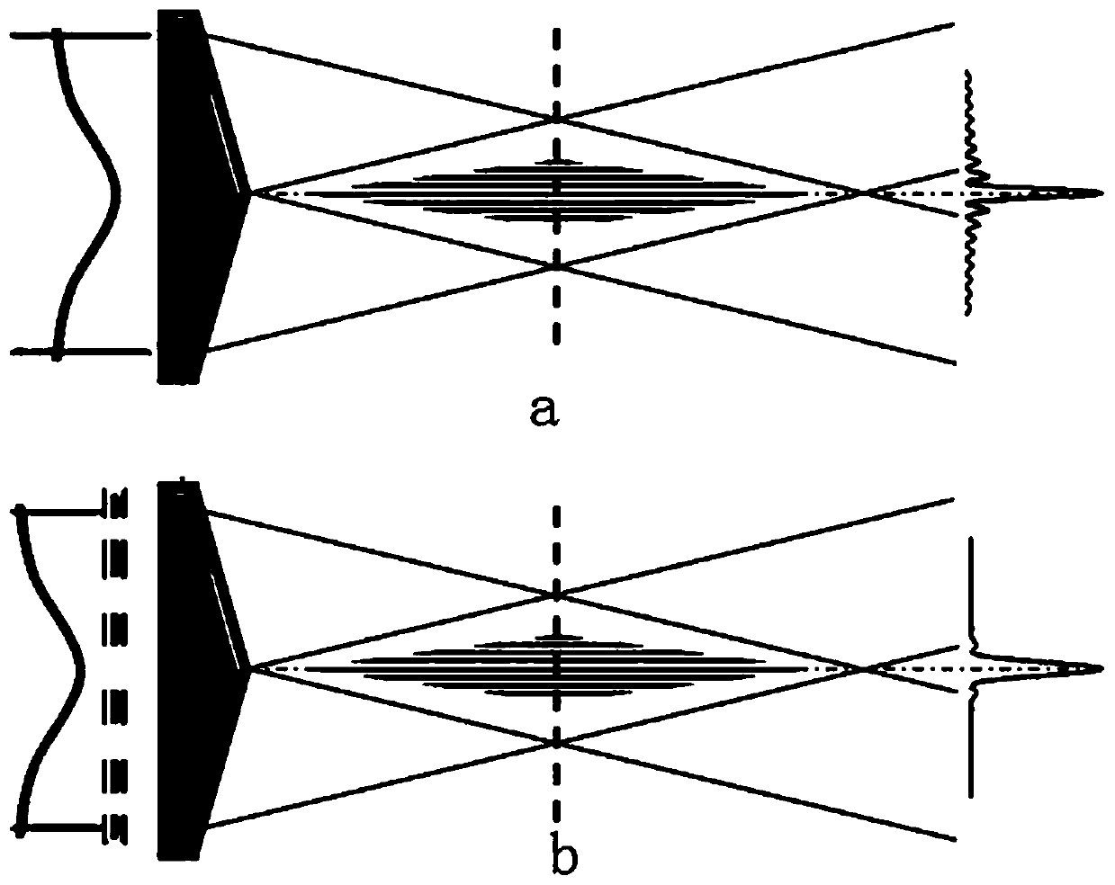
[0047] Such as figure 1 , figure 2 , Figure 4 As shown, a system for preparing a microfluidic chip by direct writing of an ultraviolet nanosecond laser includes: an ultraviolet nanosecond laser 1, an electronically controlled aperture 2 i...


PUM

PropertyMeasurementUnit
wavelengthaaaaaaaaaa
diameteraaaaaaaaaa
diameteraaaaaaaaaa

Abstract

The invention relates to an ultraviolet nanosecond laser direct-writing micro-fluidic chip preparation system and method. The micro-fluidic chip preparation system comprises an ultraviolet nanosecondlaser, an electrically controlled diaphragm, a laser beam expander, a light beam converter, a light beam rotator, a lens, a dichroscope, a laser cutting head, a three-dimensional moving platform and acontrol device. The light beam converter composed of a binary phase plate and an axicon is adopted, a smooth high-quality zero-order and large-Rayleigh-length Bessel laser can be effectively generated, a first-order aperture outside zero-order light in the center of a zero-order Bessel light beam is effectively erased, and therefore the processing quality of the Bessel light beam is effectively improved. Processing of a laser direct-writing micro-fluidic chip with a high vertical depth ratio can be achieved, the laser processing efficiency is improved, and the system is simple in structure, convenient to operate and capable of being used for high-efficiency and high-quality processing of micro-fluidic chips in various schemes.

Description

technical field [0001] The invention relates to the technical field of laser preparation, in particular to a preparation system and method for an ultraviolet nanosecond laser direct writing microfluidic chip. Background technique [0002] As one of the main means of micro-nano manufacturing, laser micro-nano processing technology has the characteristics of non-contact, low pollution and high processing precision. Laser direct writing processing is to focus the laser beam and directly expose it on the surface of the material to form a microstructure. Compared with infrared and visible light band lasers, ultraviolet lasers have lower thermal effects. With the rapid development of the ultraviolet pulse laser industry in recent years, the increase in laser power and the reduction in product prices make them more suitable for the industrialization of laser micro-nano processing systems. Successful applications have widely covered many fields such as microelectronics, materials s...

Claims


Application Information

Patent Timeline
Patent Type & Authority Applications(China)
IPC IPC(8): B23K26/364B23K26/382B23K26/70B01L3/00
CPCB01L3/502707B23K26/364B23K26/382B23K26/702
Inventor 温维佳娄凯
Owner 广州市凯佳光学科技有限公司
Why Eureka
Try Eureka