Electron beam photoetching method based on metal-doped Te-based phase change material

A technology of electron beam lithography and metal doping, applied in the field of lithography, can solve the problems of unfriendly environment, toxicity, complicated photoresist preparation process, etc., and achieve the effect of low cost and simple process

Inactive Publication Date: 2020-02-07
SUZHOU UNIV OF SCI & TECH
View PDF5 Cites 2 Cited by
  • Summary
  • Abstract
  • Description
  • Claims
  • Application Information

AI Technical Summary

Problems solved by technology

However, most of these photoresists are organic polymers, and there is some toxicity in the preparation process of photoresists, which is not friendly to the environment
In addition, the preparation process of photoresist is relatively complicated, involving the dissolution of photoresist, spin coating, baking and other steps, which is also not conducive to the electron beam lithography operation of photoresist in a vacuum environment.

Method used


Image

  • Electron beam photoetching method based on metal-doped Te-based phase change material
  • Electron beam photoetching method based on metal-doped Te-based phase change material
  • Electron beam photoetching method based on metal-doped Te-based phase change material

Examples


Embodiment 1

[0030] This embodiment provides an electron beam photoresist application and an electron beam lithography method based on a metal-doped Te-based phase change material, the steps of which include:

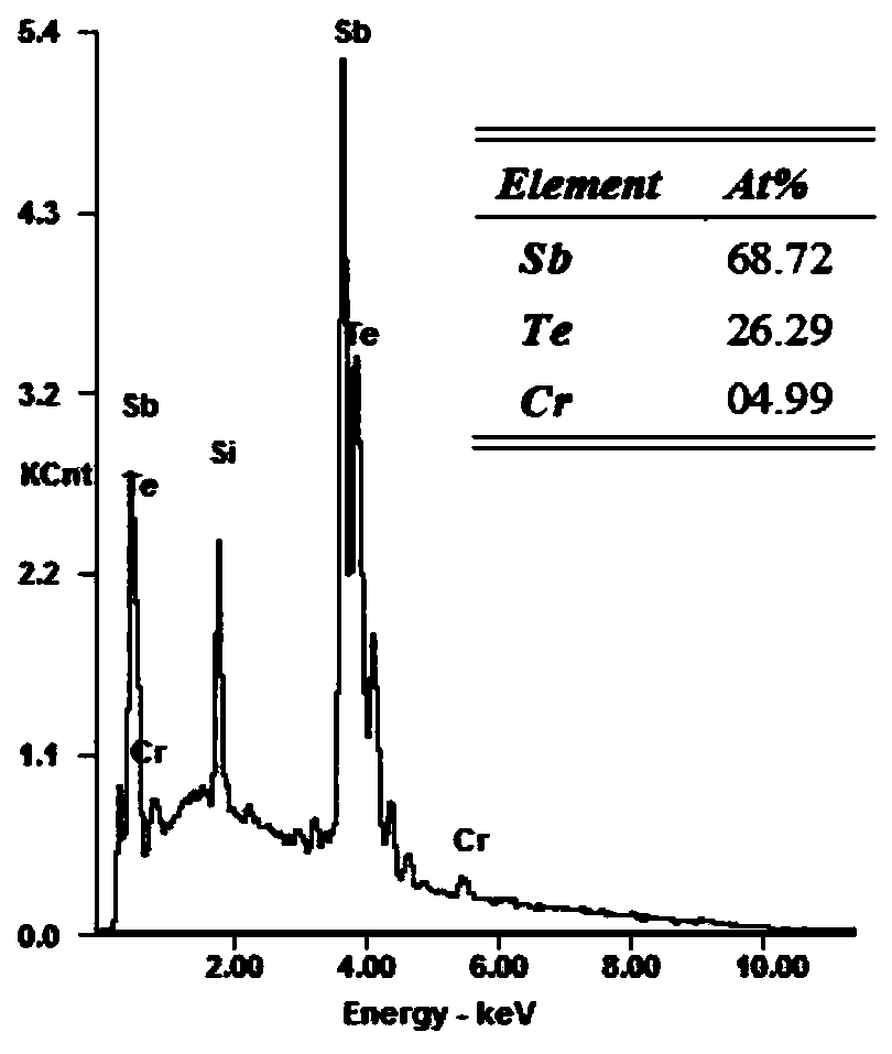
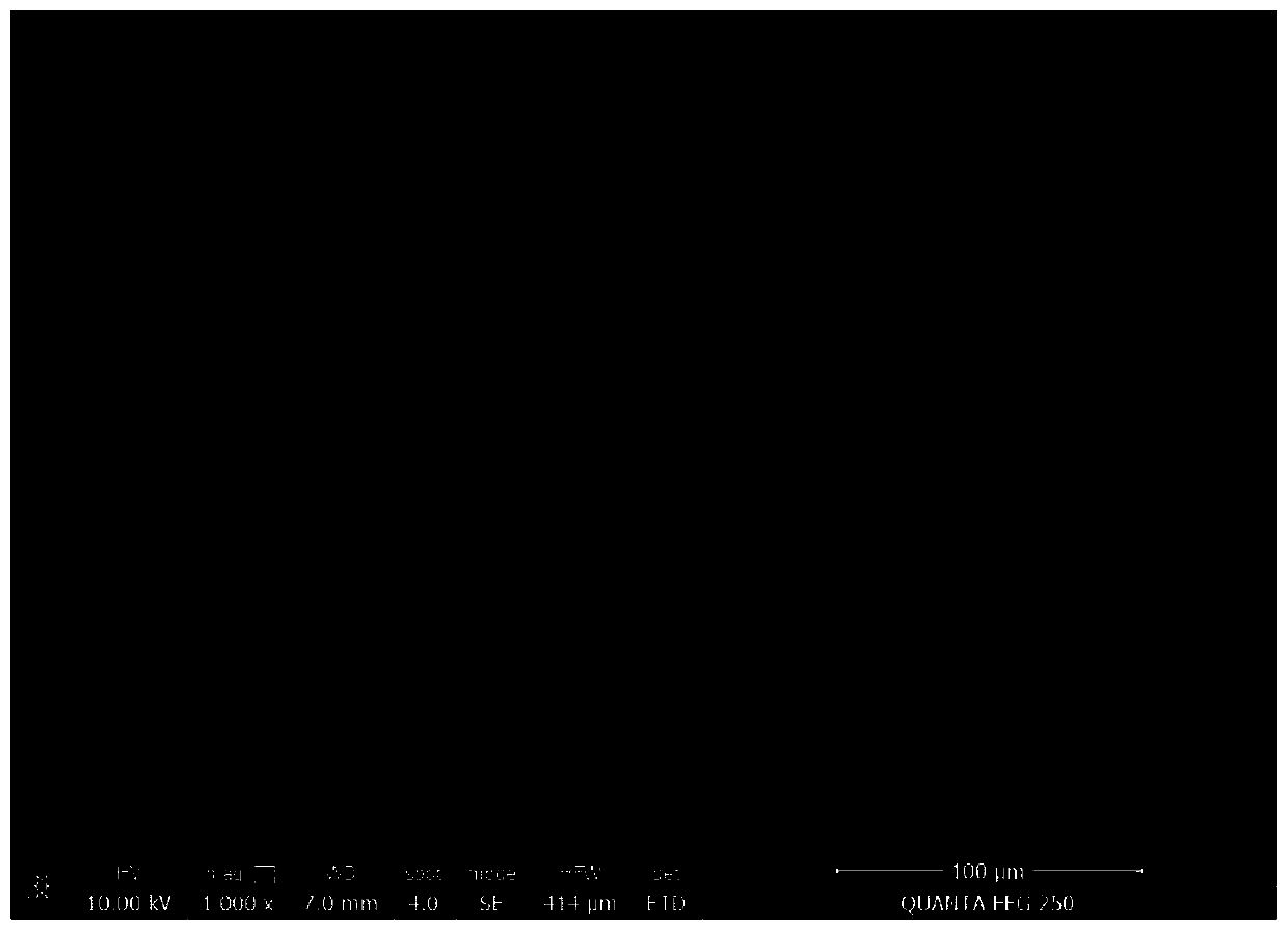
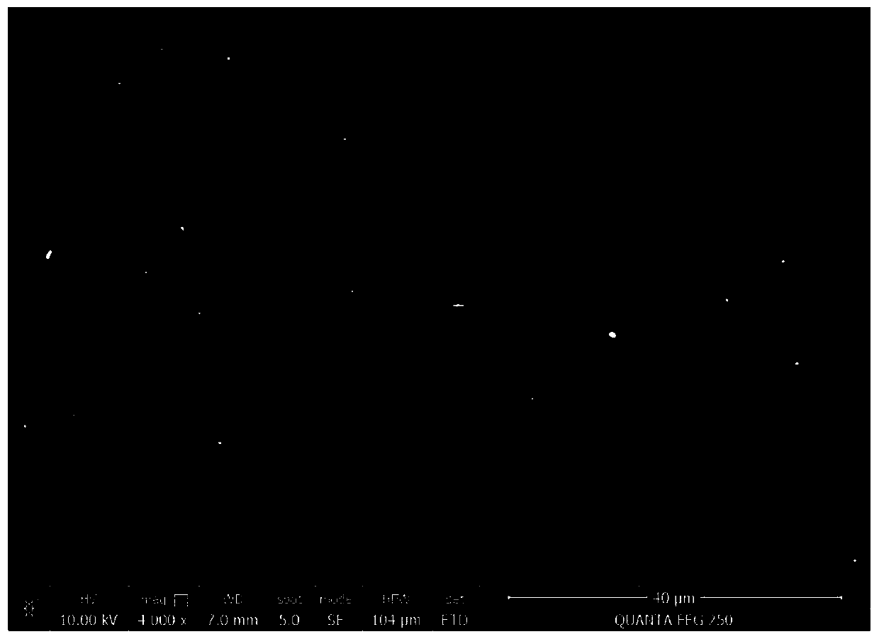
[0031] 1) Plating a layer of 100nm thick Cr-doped Sb on quartz glass by double-target magnetron co-sputtering method 2 Te film, where the background vacuum is 4×10 -4 Pa, Cr target using DC sputtering, sputtering power 4W, Sb 2 The Te target is sputtered by radio frequency, the sputtering power is 80W, the sputtering pressure is 0.5Pa, and the sputtering time is 5min; the composition of the prepared film is as follows: figure 1 Shown in the EDS result; The surface morphology of the prepared film is as follows figure 2 The SEM results are shown.

[0032] 2) Use electron beam exposure system to carry out photolithography on the above-mentioned coating samples, the acceleration voltage of the electron beam used is 10kV, the electron beam current is 1nA, and the exposure dose is 100...

Embodiment 2~4

[0034] The printing steps of Examples 2-4 are the same as those of Example 1, and the parameters of the coated samples and the photolithography parameters are shown in the table below.

[0035]

[0036]


PUM

PropertyMeasurementUnit
thicknessaaaaaaaaaa

Abstract

The invention discloses application of a metal-doped Te-based phase change material as an electron beam photoresist, and an electron beam photoetching method based on the metal-doped Te-based phase change material. The photoetching method comprises the following steps of: S1, depositing a metal-doped Te-based phase change thin film on a substrate, and S2, irradiating the phase change thin film byadopting an electron beam to crystallize the area irradiated by the electron beam so as to obtain a photoetching sample. The electron beam photoetching method based on the metal-doped Te-based phase change material is simple in process, only needs a magnetron co-sputtering method, does not need the steps of gluing, baking and the like, and is low in cost; in addition, the phase change material serving as the electron beam photoresist belongs to an environment-friendly pollution-free inorganic material; the constituent units of the phase change material are atoms, which have very low photoetching edge roughness and very high photoetching resolution.

Description

technical field [0001] The invention relates to the technical field of photolithography, in particular to an electron beam photoresist application and an electron beam photolithography method based on a metal-doped Te-based phase change material. Background technique [0002] As a nanostructure processing technology, electron beam lithography is widely used in the field of integrated circuit photomask manufacturing, and it is also widely used in nanoscience research fields such as nanoelectronics, nanooptics and low-dimensional artificial quantum structure preparation. As an important part of electron beam lithography technology, electron beam photoresist is required to be sensitive to electron beams, and polymethyl methacrylate (PMMA) is currently the most used electron beam photoresist, but PMMA photoresist There are some disadvantages during application, such as poor etching resistance, poor adhesion, poor acid and alkali resistance, and poor temperature resistance [J.Vac...

Claims


Application Information

Patent Timeline
Patent Type & Authority Applications(China)
IPC IPC(8): G03F7/20
CPCG03F7/2059
Inventor 魏涛魏劲松刘波
Owner SUZHOU UNIV OF SCI & TECH
Why Eureka
Try Eureka