Low-cost technology for preparing double electrode layer thin film transistor

A technology of thin-film transistors and electric double layers, applied in circuits, electrical components, semiconductor devices, etc., can solve the problems of high preparation costs, complex processes, unfavorable flexible industrial production, etc., and achieve low cost, flexible processes, and easy mass production Effect

Pending Publication Date: 2020-02-07
济南嘉源电子有限公司
View PDF4 Cites 2 Cited by
  • Summary
  • Abstract
  • Description
  • Claims
  • Application Information

AI Technical Summary

Problems solved by technology

[0004] As mentioned above, it has been reported that the gate and dielectric layer are patterned by simple process technology to obtain EDLTs with excellent performance. However, the source and drain electrodes of EDLTs in these reports still need to be patterned by traditional processes such as photolithography. There are problems such as complicated process, high preparation cost, and unfavorable for flexible industrial production; this patent has developed a new "Carving, cutting, and flip-chip bonding (CCFB)", which can Simultaneously realize source, drain electrode, dielectric layer, and gate electrode patterning

Method used


Image

  • Low-cost technology for preparing double electrode layer thin film transistor
  • Low-cost technology for preparing double electrode layer thin film transistor
  • Low-cost technology for preparing double electrode layer thin film transistor

Examples


Embodiment Construction

[0037] The present invention will be further described below in conjunction with the accompanying drawings and embodiments.

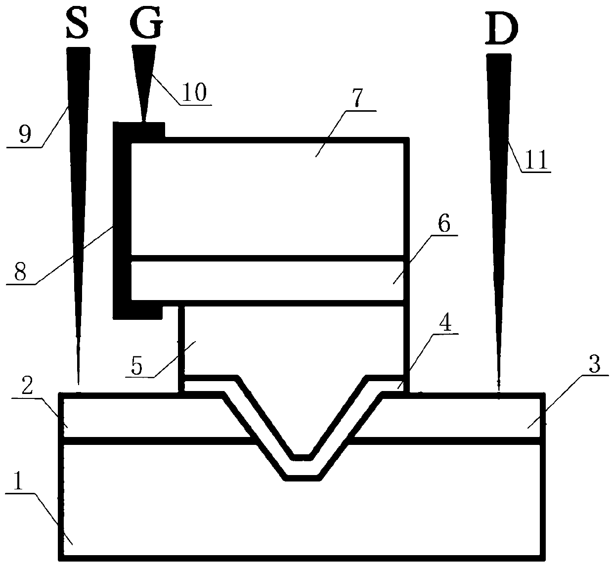
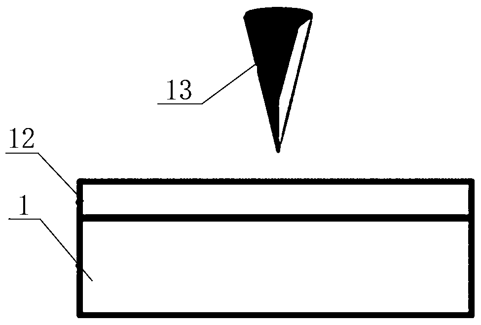
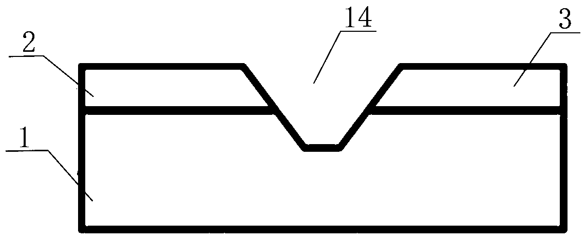
[0038] Such as figure 1 As shown, a schematic structural view of the electric double layer thin film transistor of the present invention is provided, which consists of an insulating substrate 1, a source electrode 2, a drain electrode 3, an active layer 4, a gate dielectric layer 5, a gate electrode 6, and a gate substrate The bottom 7 is composed of the source electrode 2, the drain electrode 3 and the gate electrode 6 are all made of conductive materials, the source electrode 2 and the drain electrode 3 are arranged on the insulating substrate 1, and there is a groove between the source electrode 2 and the drain electrode 3, An active layer 4 formed of semiconductor material is arranged on the trench. The gate electrode 6 is fixed on the gate substrate 7, a gate dielectric layer 5 made of electrolyte is arranged between the gate electrode 6 and the ...


PUM

PropertyMeasurementUnit
thicknessaaaaaaaaaa

Abstract

A low-cost technology for preparing a double electrode layer thin film transistor in the present invention comprises: a). substrate and electrode material selection; b). source and drain electrode patterning (carving); c). sample cleaning; d). active layer preparation; e). gate substrate and electrode material selection and gate patterning (cutting); f). gate dielectric layer preparation; and g).flip-chip bonding. According to the technology for preparing the double electrode layer thin film transistor in the present invention, a simple low-cost method for preparing a double electrode layer thin film transistor is provided, and a "carving, cutting, and flip-chip bonding (CCFB for short)" technology is developed. The technology has advantages of low costs, timesaving, environmental protection and easy large-scale production, and can be used for various substrates, for example, rigid substrates such as glass, silicon slices, mica and the like, and flexible substrate such as plastic, paper and the like. The excellent technology advantages and device performance indicate that, the technology has an extremely high application promotion prospect.

Description

technical field [0001] The invention relates to a process for preparing an electric double-layer thin film transistor, and more specifically relates to a process for preparing an electric double-layer thin film transistor mainly through scribing, slicing and flip-chip bonding. Background technique [0002] Electric Double Layer Transistors (EDLTs), because its gate dielectric is an electrolyte rich in mobile ions, the ions of the electrolyte drift directionally under the action of an external gate voltage, and at the gate dielectric / semiconductor layer interface An electric double layer with a thickness of only about 1 nm is induced at , so the electric double layer has a very high capacitance value, usually > 1 µF / cm 2 . Therefore EDLTs can achieve low voltage operation and high current output. In recent years, there have been many research reports on EDLTs at home and abroad. Common patterning techniques include photolithography, printing (such as screen printing, hi...

Claims


Application Information

Patent Timeline
Patent Type & Authority Applications(China)
IPC IPC(8): H01L21/336
CPCH01L29/66742
Inventor 辛倩杜路路宋爱民杜军
Owner 济南嘉源电子有限公司
Why Eureka
Try Eureka