Circularly polarized reconfigurable antenna integrated with adjustable phase-shifting power divider

A technology for reconstructing antennas and power dividers, which is applied to antennas, folded antennas, and the structural connection of antenna grounding switches, etc., can solve problems such as difficulty in meeting high speed and high precision, difficulty in antenna processing and manufacturing, and large insertion loss of photoconductive switches. Achieve the effect of simple structure, easy processing and fabrication, and low insertion loss

Active Publication Date: 2020-02-11
XIDIAN UNIV
14 Cites 2 Cited by

AI-Extracted Technical Summary

Problems solved by technology

[0004] Reconfigurable circularly polarized antennas usually use mechanical, optical, and electronic methods to adjust the working state of the antenna. The mechanical method uses actuators and other actuators to adjust the shape and structure of the antenna, and the adjustment range is large. However, it needs Additional mechanical devices, while difficult to meet the requirements of high speed and high precision
The optical method is to change the current distribution on the surface of the antenna by controlling the on-off state of the photoconductive switch. The response speed is fast and easy to contr...

Abstract

The invention relates to a circularly polarized reconfigurable antenna integrated with an adjustable phase-shifting power divider. The antenna includes a first dielectric substrate, a second dielectric substrate, the adjustable phase-shifting power divider, a grounded metal plate, a main radiation sheet, and a parasitic radiation sheet. The adjustable phase-shifting power divider and the ring-shaped main radiation sheet are printed on the upper surface of the first dielectric substrate. The grounded metal plate is printed on the lower surface of the first dielectric substrate. The second dielectric substrate is a cylinder, and the parasitic radiation sheet is printed on the upper surface thereof. The adjustable phase-shifting power divider is connected with the main radiation sheet. The first dielectric substrate is separated from the second dielectric substrate and fixed by a plurality of insulating studs. The circularly polarized reconfigurable antenna integrated with the adjustablephase-shifting power divider, which is provided by the invention, has the advantages that (1) the characteristics of left-handed circular polarization and right-handed circular polarization are realized under the same antenna aperture, and the antenna has a circularly polarized reconfigurable function; (2) the switching speed is fast; the insertion loss is small; the control is simple; and (3) theantenna is easy to process and manufacture, and low in cost.

Application Domain

Collapsable antennas meansRadiating elements structural forms +1

Technology Topic

Dielectric substrateInsertion loss +6

Image

  • Circularly polarized reconfigurable antenna integrated with adjustable phase-shifting power divider
  • Circularly polarized reconfigurable antenna integrated with adjustable phase-shifting power divider
  • Circularly polarized reconfigurable antenna integrated with adjustable phase-shifting power divider

Examples

  • Experimental program(1)

Example Embodiment

[0039] The specific embodiments of the present invention will be described in detail below.
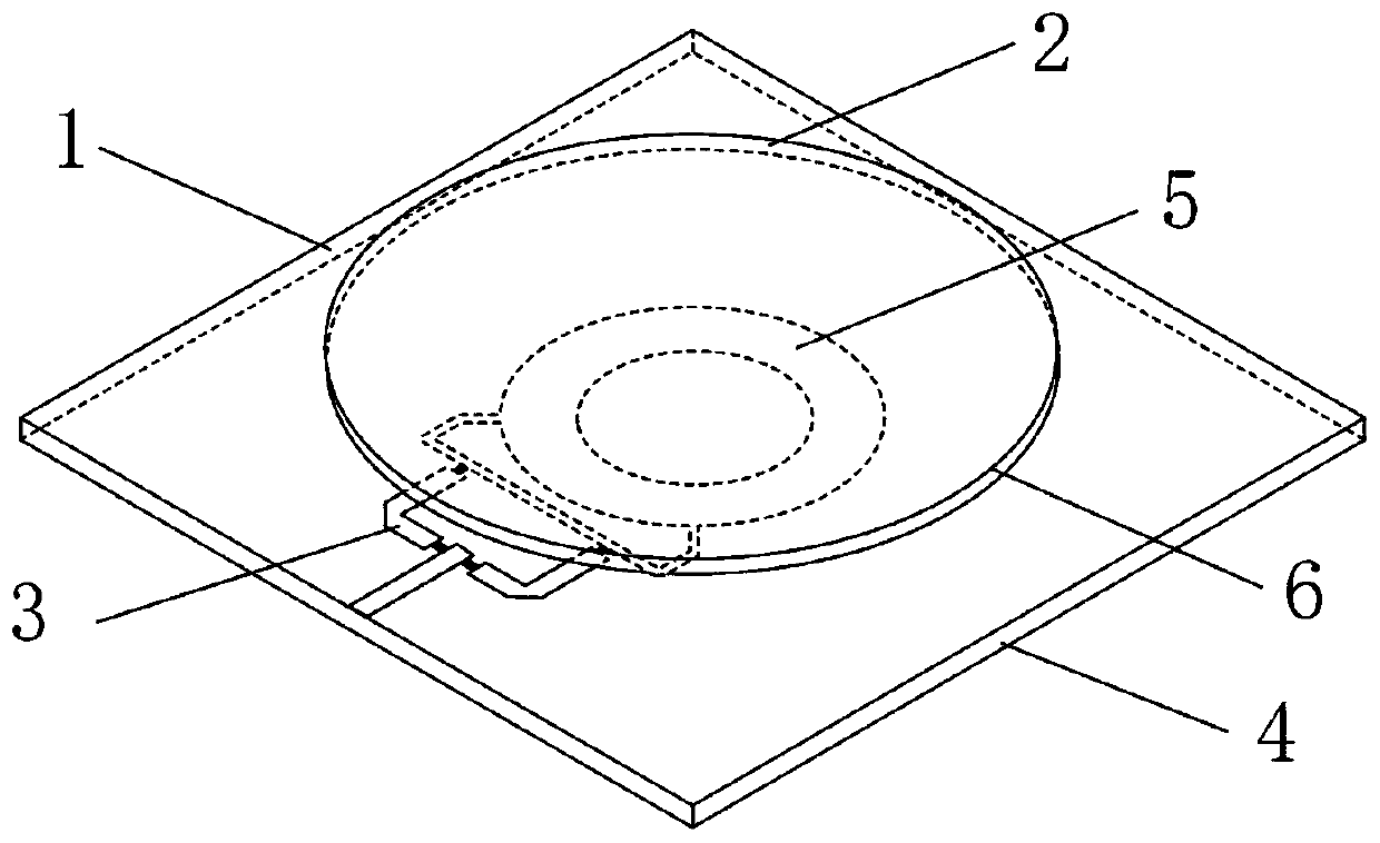
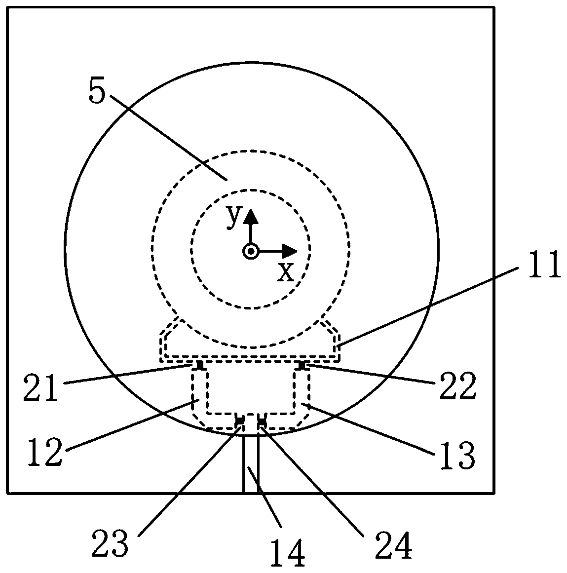
[0040] like figure 1 and figure 2 As shown in the figure, a circularly polarized reconfigurable antenna integrating an adjustable phase-shifting power divider includes a first dielectric substrate 1, a second dielectric substrate 2, an adjustable phase-shifting power divider 3, a grounded metal plate 4, a main Radiation sheet 5 and parasitic radiation sheet 6, where:
[0041] The first dielectric substrate 1 is made of a cuboid dielectric material with a relative dielectric constant of 3.5, a thickness of 1 mm, and a length and width of 70 mm. The upper surface of the first dielectric substrate 1 is printed with an adjustable phase-shifting power divider 3 and The annular main radiating sheet 5 (inner diameter is 8.9mm, outer diameter is 14.2mm.), the lower surface of the first dielectric substrate 1 is printed with a grounding metal plate 4 that completely overlaps with it;
[0042] The second dielectric substrate 2 is made of a cylindrical dielectric material with a relative permittivity of 4.4 and a thickness of 0.8 mm, and its radius is 26.9 mm. The upper surface of the second dielectric substrate 2 is printed with a parasitic radiation sheet 6 that completely overlaps with the upper surface. ;
[0043] The adjustable phase-shift power divider 3 is connected to the main radiator 5;
[0044] The first dielectric substrate 1 is separated from the second dielectric substrate 2 and fixed by a plurality of studs.
[0045] Further, the adjustable phase-shift power divider 3 includes four microstrip lines and four radio frequency switches for generating two output signals with equal amplitude and adjustable phase difference, and feeding the output signals into the main radiator 5, of which:
[0046] The four microstrip lines are the first microstrip line 11 , the second microstrip line 12 , the third microstrip line 13 and the fourth microstrip line 14 respectively, and the four radio frequency switches are the first radio frequency switch 21 and the second radio frequency switch respectively The switch 22 , the third radio frequency switch 23 and the fourth radio frequency switch 24 .
[0047] Further, the characteristic impedance of the first microstrip line 11 is 100 ohms, and both ends of the first microstrip line 11 are bent and connected to the main radiating sheet 5 respectively for feeding. The included angle between the two straight lines is 90°; the characteristic impedances of the second microstrip line 12, the third microstrip line 13 and the fourth microstrip line 14 are all 50 ohms,
[0048] The connection between the first microstrip line 11 and the second microstrip line 12 , the connection between the first microstrip line 11 and the third microstrip line 13 , and the connection between the second microstrip line 12 and the fourth microstrip line 14 , an opening is etched at the connection between the third microstrip line 13 and the fourth microstrip line 14, wherein:
[0049]A first radio frequency switch 21 is provided at the opening at the connection between the first microstrip line 11 and the second microstrip line 12;
[0050] A second radio frequency switch 22 is provided at the opening at the connection between the first microstrip line 11 and the third microstrip line 13;
[0051] The opening at the connection of the second microstrip line 12 and the fourth microstrip line 14 is provided with a third radio frequency switch 23;
[0052] The opening at the connection of the third microstrip line 13 and the fourth microstrip line 14 is provided with a fourth radio frequency switch 24 .
[0053] Further, the second microstrip line 12 and the third microstrip line 13 are L-shaped microstrip lines with the same size and shape and are mirror-symmetrical about the center of the ring of the main radiator 5, and the fourth microstrip line 14 is a rectangular microstrip. Wire.
[0054] Further, the first radio frequency switch 21 and the third radio frequency switch 23 form a group, the second radio frequency switch 22 and the fourth radio frequency switch 24 form a group, and the adjustable phase shift can be controlled by controlling the on-off of each radio frequency switch. The phase difference between the two output signals of the power divider 3 is 90° or -90°.
[0055] When the first RF switch 21 and the third RF switch 23 are turned off, and the second RF switch 22 and the fourth RF switch 24 are turned on, the amplitudes of the left and right output signals of the adjustable phase-shift power divider 3 are equal, And the phase difference generated by subtracting the left-circuit feed phase from the right-circuit feed phase is -90°, so that the antenna realizes the characteristic of left-hand circular polarization; when the first radio frequency switch 21 and the third radio frequency switch 23 are turned on, the second radio frequency When the switch 22 and the fourth radio frequency switch 24 are disconnected, the amplitudes of the left and right output signals of the adjustable phase-shift power divider 3 are equal, and the phase difference generated by subtracting the left feed phase from the right feed phase is: 90°, so that the antenna realizes the characteristic of right-hand circular polarization. Switching between left-hand circular polarization and right-hand circular polarization can be achieved by changing the on-off state of the radio frequency switch.
[0056] Further, the distance between the first radio frequency switch 21 and the second radio frequency switch 22 is 16.6 mm, which is approximately equal to λ g /4(λ g is the working wavelength corresponding to 2.45GHz).
[0057] Furthermore, the first radio frequency switch 21 , the second radio frequency switch 22 , the third radio frequency switch 23 , and the fourth radio frequency switch 24 are all PIN diode switches.
[0058] Further, the distance between the first dielectric substrate 1 and the second dielectric substrate 2 is 5 mm (that is, the second dielectric substrate 2 is located on the same horizontal plane with a height of 5 mm above the first dielectric substrate 1 ).
[0059] Below in conjunction with the simulation experiment, the technical effect of the present invention is further described:
[0060] like image 3 and Figure 4 As shown, when working in the left-handed circular polarization and right-handed circular polarization state, the reflection coefficient of the antenna in the frequency range of 2.29GHz to 2.61GHz is less than -10dB, and the reflection coefficient in the frequency range of 2.35GHz to 2.58GHz is less than -10dB. The axial ratio is less than 3dB.
[0061] like Figure 5a , Figure 5b , Figure 6a and Figure 6b As shown, when working in the left-handed circular polarization state, the maximum gain of the antenna in the radiation pattern at 2.45 GHz in the embodiment can reach 7.92 dBi; when working in the right-handed circularly polarized state, the antenna in the embodiment is at 2.45 dBi The maximum gain in the GHz radiation pattern can reach 7.88dBi. In the above two states, the antenna also has lower cross-polarization and higher front-to-back ratio.
[0062] The embodiments of the present invention have been described in detail above. However, the present invention is not limited to the above-mentioned embodiments, and various changes can be made within the scope of knowledge possessed by those skilled in the art without departing from the spirit of the present invention.

PUM

no PUM

Description & Claims & Application Information

We can also present the details of the Description, Claims and Application information to help users get a comprehensive understanding of the technical details of the patent, such as background art, summary of invention, brief description of drawings, description of embodiments, and other original content. On the other hand, users can also determine the specific scope of protection of the technology through the list of claims; as well as understand the changes in the life cycle of the technology with the presentation of the patent timeline. Login to view more.

Similar technology patents

Shield gate groove type field effect transistor with low on-resistance and preparation method thereof

PendingCN114744038Aeasy to run outFast switching speed
Owner:无锡先瞳半导体科技有限公司

Dynamic continuous stress-free acquisition system and method for goose body quality data

PendingCN111121933Aavoid stress responseFast switching speed
Owner:YANGZHOU UNIV

Television control method and device based on fingerprint identification, equipment and storage medium

PendingCN113691868AReduce the difficulty of operationFast switching speed
Owner:NANJING SKYWORTH INST OF INFORMATION TECH CO LTD

Ultralow-temperature noise source assembly

PendingCN111900936ANoise output is stableFast switching speed
Owner:CHINA ELECTRONICS TECH GROUP CORP NO 16 INST

Method for realizing mobile node switching in mobile IP

InactiveCN1324924Csave judgment timeFast switching speed
Owner:BEIHANG UNIV

Classification and recommendation of technical efficacy words

  • Fast switching speed
  • low insertion loss

Method and system for switching of network television channels

InactiveCN104602115AFast switching speedshorten the time
Owner:HISENSE BROADBAND MULTIMEDIA TECH

Method and device for switching working mode of PIR camera

ActiveCN105491285AFast switching speed
Owner:ZHEJIANG UNIVIEW TECH

Programmable optical filter capable of realizing any spectrum transmittance

InactiveCN107144960AFast switching speedeasy to operate
Owner:NORTHEASTERN UNIV

Optical modulator

ActiveUS20130011093A1low insertion lossattenuation of intensity be low
Owner:NIPPON TELEGRAPH & TELEPHONE CORP

Transmit-receive switching mechanism for TDD radio communication system

InactiveCN101282127Aprevent self-oscillationlow insertion loss
Owner:马瑞花 +5

Quasi-distributed sea water temperature salinity sensor, measuring device and method thereof

ActiveCN106932026ALow loss characteristiclow insertion loss
Owner:HUAZHONG UNIV OF SCI & TECH

Microstrip device test system

InactiveCN104849593Alow insertion lossSmall standing wave
Owner:UNIV OF ELECTRONIC SCI & TECH OF CHINA

Microstrip dual-mode filter with features of wide stop band and low spurious

ActiveCN101667671AIncreased spurious suppression and stopband widthlow insertion loss
Owner:SOUTHEAST UNIV
Why Eureka
Try Eureka