A composition-tunable inorganic perovskite photoelectric thin film and its low-temperature preparation method and device application

A technology of optoelectronic thin film and inorganic calcium, which is applied in the field of controllable preparation of new semiconductor optoelectronic materials and devices, can solve the problems of poor optoelectronic properties, low solubility, and reduced conductivity of perovskite materials, and achieves accurate and adjustable halogen ratio, optical Bandgap Tunable Effects

Active Publication Date: 2021-02-05
JINAN UNIVERSITY
View PDF8 Cites 0 Cited by
  • Summary
  • Abstract
  • Description
  • Claims
  • Application Information

AI Technical Summary

Problems solved by technology

[0004] In order to solve the current CsPbCl x Br 3-x In the process of preparing perovskite thin films, there are problems such as low solubility and poor photoelectric properties, that is, the raw materials CsCl and PbCl 2 Very insoluble in DMSO or DMF solvents and the introduction of a large number of functional groups during the preparation process leads to a decrease in the conductivity of the perovskite material

Method used


Image

  • A composition-tunable inorganic perovskite photoelectric thin film and its low-temperature preparation method and device application
  • A composition-tunable inorganic perovskite photoelectric thin film and its low-temperature preparation method and device application
  • A composition-tunable inorganic perovskite photoelectric thin film and its low-temperature preparation method and device application

Examples


Embodiment 1

[0048] The transparent conductive substrate (ITO / FTO) was ultrasonically cleaned with deionized water, acetone, and isopropanol, respectively, and ultrasonically oscillated in the respective solutions for 15 minutes.

[0049] The above cleaned substrates were washed with N 2 Blow dry for use, and use ultraviolet ozone to clean the surface of the transparent conductive substrate for 20 minutes.

[0050] Preparation of cesium lead bromine perovskite thin film: 0.4 mol of cesium bromide and 0.4 mol of lead bromide were dissolved in 1 mL of DMSO solution, followed by heating and stirring for 12 hours at a heating temperature of 70°C.

[0051] The prepared precursor solution was spin-coated on the FTO substrate. The spin-coating conditions were: 500 rpm for 6 seconds, and 5000 rpm for 30 seconds; then it was annealed at 100 °C in a nitrogen atmosphere for 10 minutes.

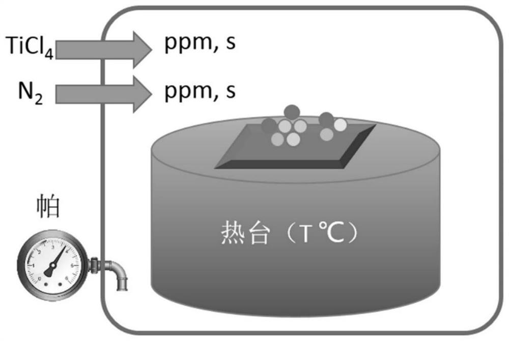
[0052] Finally, TiCl was purged on the spin-coated perovskite substrate by atomic layer deposition 4 , the depos...

Embodiment 2

[0056] The flexible conductive substrates (such as PET / ITO) were ultrasonically cleaned with deionized water, acetone, and isopropanol, respectively, and ultrasonically cleaned in the respective solutions for 15 min.

[0057] The above cleaned substrate was blown dry with nitrogen, and treated with ultraviolet ozone for 20 minutes.

[0058] The inorganic perovskite precursor solution prepared in Example 1 was spin-coated on the flexible ITO substrate. The spin-coating conditions were: 6 seconds at a rotation speed of 500 rpm, and then 30 seconds at a rotation speed of 5000 rpm; then it was annealed at 100 ° C under a nitrogen atmosphere treatment, the annealing time is 10min.

[0059] Finally, TiCl was purged on the spin-coated perovskite substrate by atomic layer deposition 4 , the deposition conditions are: precursor source selection (titanium tetrachloride, TiCl 4 ), TiCl 4 The time to enter the pipeline is 500ms, the cavity temperature is set at 105°C, 1-100 cycles, the...

Embodiment 3

[0060] Embodiment 3 The making of photodetection device

[0061] Use deionized water, acetone, and isopropanol to ultrasonically clean the hard substrate or flexible conductive substrate (such as PET / ITO), respectively, and ultrasonically clean them in their respective solutions for 15 minutes.

[0062] The above cleaned substrate was blown dry with nitrogen, and treated with ultraviolet ozone for 20 minutes.

[0063] Deposit a layer of titanium oxide on the above treated substrate by atomic layer deposition technology, deposition conditions: chamber temperature 105°C, time for titanium tetrachloride to flow into the pipeline is 200ms, purge for 2 seconds, time for water to flow into the pipeline is 500ms, purge for 4 seconds, and the number of cycles is set to 170 cycles.

[0064] The inorganic perovskite precursor solution prepared in Example 1 was spin-coated on the above-mentioned substrate, and the spin-coating conditions were: 6 seconds at a rotation speed of 500 rpm, a...


PUM

PropertyMeasurementUnit
thicknessaaaaaaaaaa

Abstract

The invention belongs to the technical field of preparation of novel semiconductor materials and devices, and particularly discloses a component-adjustable inorganic perovskite thin film and a low-temperature preparation method and device application thereof. The preparation method comprises the following steps of: dissolving CsX and AB in an organic solvent and uniformly stirring to obtain a precursor solution, spin-coating the obtained precursor on a conductive substrate, and then annealing the prepared film, and then transferring the sample to an atomic deposition system for ion exchange reaction to obtain the inorganic perovskite photoelectric thin film with accurate and adjustable components, and successfully applying the inorganic perovskite photoelectric thin film to a photovoltaicdevice. According to the method, the problem of low solubility traditionally is solved, the uniformity and the compactness of the thin film are improved, the atomic layer deposition temperature is farlower than 200 DEG C, the method is suitable for a hard substrate and a flexible substrate, and accurate regulation and control of the proportion of inorganic perovskite halogen elements are better facilitated; in addition, the precursors are all inorganic matters, so that the problem of poor conductivity of the thin film is solved, and the method has important significance in inorganic perovskite thin film preparation and device application.

Description

technical field [0001] The invention belongs to the technical field of controllable preparation of novel semiconductor optoelectronic materials and devices, and in particular relates to a composition-tunable inorganic perovskite photoelectric thin film and its low-temperature preparation method and device application. Background technique [0002] In recent years, organic / inorganic hybrid halide perovskite materials have shown outstanding photoelectric conversion efficiency due to their excellent properties such as high light absorption coefficient and long diffusion distance; they are widely used in solar cells, photodetectors, light-emitting diodes, etc. field. However, the poor light, thermal and humidity stability of hybrid perovskite materials greatly limits their wide application in the field of optoelectronics. It is gratifying that inorganic perovskite optoelectronic materials such as CsMX 3 (M=Pb, Bi, Sn, X=Cl, Br, I)), in addition to having similar photoelectric ...

Claims


Application Information

Patent Timeline
Patent Type & Authority Patents(China)
IPC IPC(8): H01L31/18H01L31/032
CPCH01L31/032H01L31/18Y02P70/50
Inventor 赵传熙麦文杰岑国标赵志娟
Owner JINAN UNIVERSITY
Why Eureka
Try Eureka