
GaN-based completely-vertical Schottky varactor based on metal eave structure and preparation method thereof

A varactor and Schottky contact technology, which is applied in semiconductor/solid-state device manufacturing, electrical components, circuits, etc., can solve the problems of low output power and frequency multiplication conversion efficiency, low electron mobility, breakdown voltage and leakage current There is a large gap with the theoretical value, etc., to achieve the effect of eliminating the impact

Active Publication Date: 2020-02-18
NAT SPACE SCI CENT CAS
View PDF6 Cites 2 Cited by
  • Summary
  • Abstract
  • Description
  • Claims
  • Application Information

AI Technical Summary

Problems solved by technology

[0004] At present, 110G frequency multiplier circuits based on GaN Schottky diodes have been reported. Due to the low electron mobility of GaN materials, the series resistance of Schottky diodes is relatively large; although GaN materials have extremely high breakdown field strength, the currently developed The breakdown voltage and leakage current of GaN-based Schottky varactors are far from the theoretical values, resulting in low output power and frequency conversion efficiency

Method used


Image

  • GaN-based completely-vertical Schottky varactor based on metal eave structure and preparation method thereof
  • GaN-based completely-vertical Schottky varactor based on metal eave structure and preparation method thereof
  • GaN-based completely-vertical Schottky varactor based on metal eave structure and preparation method thereof

Examples


Embodiment 1

[0037] A method for preparing a GaN-based complete vertical Schottky varactor based on a metal eaves structure, the preparation method comprising the steps of:

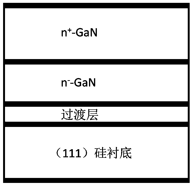
[0038] 1. If figure 1 As shown, lightly doped / heavily doped GaN epitaxial wafers with Si substrates with a diameter of 2 inches were selected. The epitaxial wafer structure from top to bottom is as follows: the doping concentration is greater than 5E18 / cm 3 The 3um~5um heavily doped layer (n+), the doping concentration is 3E16~2E17 / cm 3 300-500nm lightly doped layer (n-), transition layer (transition layer), Si substrate (Substrate);

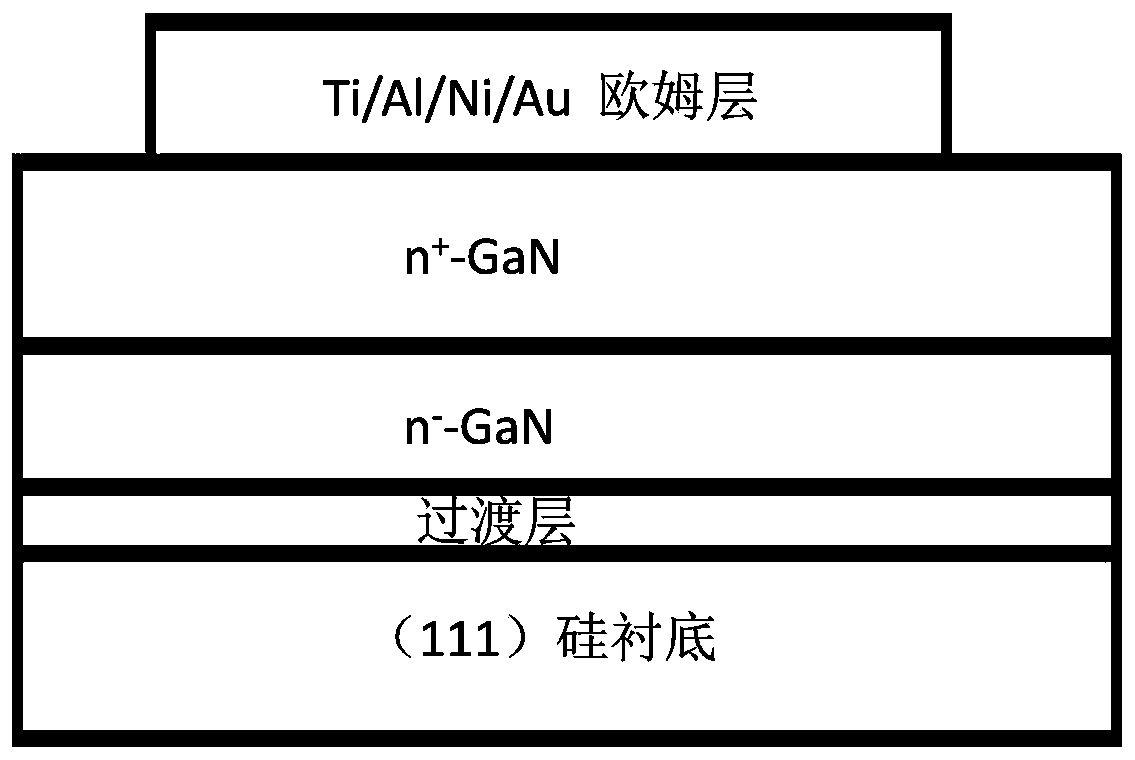
[0039] 2. Ohmic metal evaporation: such as figure 2 shown, in n + -Using electron beam evaporation Ti / Al / Ni / Au on the GaN layer as the cathode (ohmic metal layer) of the device, followed by N 2 Rapid thermal annealing treatment at 850°C for 30s under ambient conditions;

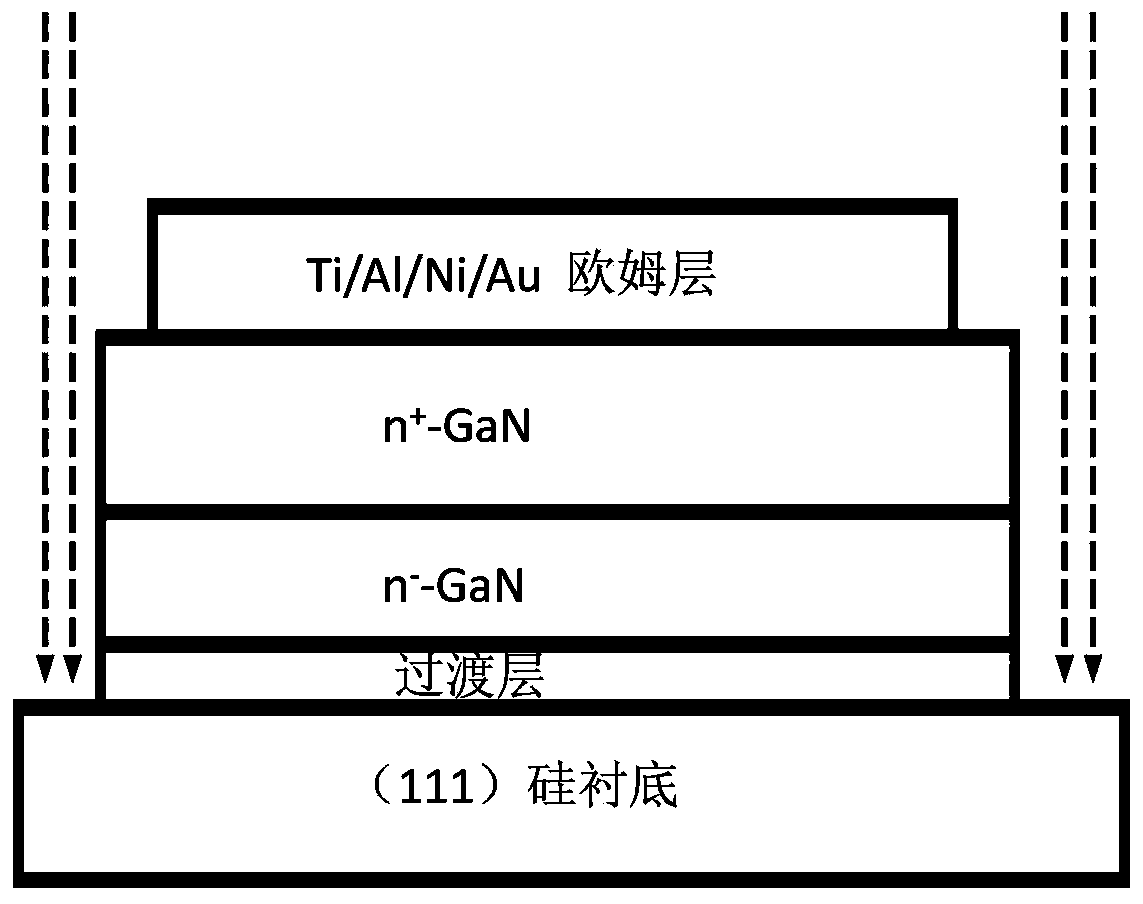
[0040] 3. Evaporation of bonding metal Au: Evaporate another layer on the ohmic metal layer with a thickness...


PUM

PropertyMeasurementUnit
Doping concentrationaaaaaaaaaa
Thicknessaaaaaaaaaa
Doping concentrationaaaaaaaaaa

Abstract

The invention discloses a GaN-based completely-vertical Schottky varactor based on a metal eave structure and a preparation method thereof. The varactor structurally comprises a silicon substrate layer; a substrate protection layer, a bonding layer, an ohmic metal layer, an n<+>-GaN layer, an n<->-GaN layer and a Schottky contact metal layer are sequentially arranged on the silicon substrate layerfrom bottom to top; an anode pad is arranged on the Schottky contact metal layer; and a cathode pad in contact with the bonding layer is further arranged on the bonding layer. The reverse bias characteristic is effectively improved, which is reflected by the increase of reverse breakdown voltage and the reduction of leakage current during reverse bias, so that the frequency multiplication efficiency is effectively improved.

Description

technical field [0001] The invention relates to the field of semiconductor devices, in particular, the invention relates to a GaN-based complete vertical Schottky varactor based on a metal eaves structure and a preparation method thereof. Background technique [0002] Terahertz (THz) waves are electromagnetic waves with a frequency in the range of 0.3THz to 3THz. Due to the particularity of the THz source: the high frequency based on electronic methods and the low frequency based on optical methods are not easy to achieve. Until the 1920s, The advantages of terahertz waves and the research of terahertz technology have gradually attracted people's attention. Terahertz wavelength is very short, it is a good broadband information carrier, and has great application prospects in the fields of high-resolution spectroscopy, imaging systems, and communications; terahertz waves can penetrate biological tissues and will not cause harmful ionization to biological cells , so it is espe...

Claims


Application Information

Patent Timeline
IPC IPC(8): H01L29/93H01L29/872H01L21/329
CPCH01L29/93H01L29/872H01L29/66143Y02P70/50
Inventor 祁路伟张德海孟进
Owner NAT SPACE SCI CENT CAS
Learn More