Etching solution for etching indium tin oxide semiconductor transparent conductive film

A technology of transparent conductive film and indium tin oxide, which is applied in surface etching compositions, chemical instruments and methods, etc., can solve the problem of difficulty in controlling the etching angle and the etching amount of the metal layer, affecting the repeatability of the effect, and unreasonable formula settings. and other problems, to achieve the effect of rapid and complete biodegradation, clear line edges without side etching, and stable etching effect

Inactive Publication Date: 2020-03-06
SUZHOU BOYANG CHEM
View PDF11 Cites 3 Cited by
  • Summary
  • Abstract
  • Description
  • Claims
  • Application Information

AI Technical Summary

Problems solved by technology

The existing etching solution has unreasonable formula settings, so that the quality of the etching solution itself has certain defects. For example, the Chinese invention patent with the application publication number of CN102732253A discloses a kind of this etching solution, and the composition of the etching solution is hydrochloric acid or nitric acid, FeCl 3 , nitrate compound or chlorine-based compound, surfactant and pure water, the surfactant is a mixture of anionic surfactant and polyoxyethylene nonionic surfactant
In the process of etching ITO material, the above etching solution contains FeCl 3 The reason is that the etching speed is too fast, and the amount of side etching is large, the etching solution is unstable, and it is difficult to control the etching angle and the etching amount of the metal layer, which affects the repeatability of the effect

Method used


Image

  • Etching solution for etching indium tin oxide semiconductor transparent conductive film
  • Etching solution for etching indium tin oxide semiconductor transparent conductive film
  • Etching solution for etching indium tin oxide semiconductor transparent conductive film

Examples


Embodiment 1

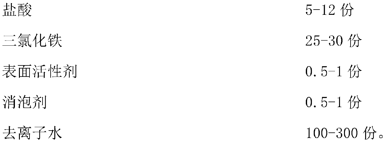
[0017] An etchant for etching transparent conductive films of indium tin oxide semiconductors, characterized in that, calculated in parts by weight, comprising:

[0018]

[0019] Etch the ITO film of the product of this example, and it will be etched clean at 25°C for 1 minute, with complete graphics, no damage to the photoresist, and good protection of the etched lines. Nothing changes within the segment.

Embodiment 2

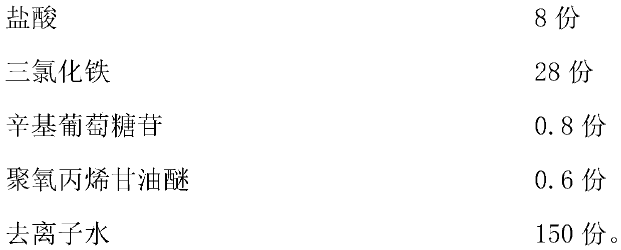
[0021] An etchant for etching transparent conductive films of indium tin oxide semiconductors, characterized in that, calculated in parts by weight, comprising:

[0022]

[0023] Etch the ITO film of the product of this example, and it will be etched clean after 3 minutes at 25°C, with complete graphics, no damage to the photoresist, and good protection of the etched lines. Nothing changes within the segment.

Embodiment 3

[0025] An etchant for etching transparent conductive films of indium tin oxide semiconductors, characterized in that, calculated in parts by weight, comprising:

[0026]

[0027] The product of this example is etched on the ITO film, and it is etched clean at 25°C for 6 minutes. Nothing changes within the segment.


PUM

PropertyMeasurementUnit
electrical resistivityaaaaaaaaaa

Abstract

The invention discloses an etching solution for etching an indium tin oxide semiconductor transparent conductive film, wherein the etching solution comprises the components in parts by weight: 5-12 parts of hydrochloric acid, 25-30 parts of ferric trichloride, 0.5-1 part of a surfactant, 0.5-1 part of a defoaming agent and 100-300 parts of deionized water. The etching solution has the beneficial effects that the alkyl polyglycoside surfactant has the advantages of low surface tension, no cloud point, strong wetting power, strong compatibility, no toxicity, no harm, no irritation to skin, and rapid and thorough biodegradation, the surface tension of the ITO etching solution is effectively reduced, and the etching speed is moderate in the etching process; the defoaming agent can eliminate foam generated by alkyl polyglycoside surfactants in the etching process, the high-precision processing requirement of ITO film etching is met, the photoresist is not damaged, etching lines are well protected, patterns are complete, etching is thorough within 1 min at the temperature of 25 DEG C, the etching effect is stable, and the repeatability is good.

Description

technical field [0001] The invention relates to the technical field of chemical preparations, in particular to an etchant for etching transparent conductive films of indium tin oxide semiconductors. Background technique [0002] Etching solution is widely used in the etching of transparent conductive film (ITO film), which is convenient for the application of transparent conductive film (ITO film). The existing etching solution has unreasonable formula settings, so that the quality of the etching solution itself has certain defects. For example, the Chinese invention patent with the application publication number of CN102732253A discloses a kind of this etching solution, and the composition of the etching solution is hydrochloric acid or nitric acid, FeCl 3 , nitrate compound or chlorine-based compound, surfactant and pure water, and the surfactant is a mixture of anionic surfactant and polyoxyethylene nonionic surfactant. In the process of etching ITO material, the above ...

Claims


Application Information

Patent Timeline
Patent Type & Authority Applications(China)
IPC IPC(8): C09K13/06
CPCC09K13/06
Inventor 王润杰陈浩卢洪庆严増源
Owner SUZHOU BOYANG CHEM
Why Eureka
Try Eureka