Manufacturing method of back contact heterojunction solar cell with double-sided power generation

A technology of a solar cell and a manufacturing method, which is applied in the field of solar cells, can solve the problems of power generation without any advantage and can only generate electricity from one side, and achieves the effects of increasing the power generation of modules, improving quality and improving quality.

Inactive Publication Date: 2020-03-20
GOLD STONE (FUJIAN) ENERGY CO LTD
View PDF3 Cites 4 Cited by
  • Summary
  • Abstract
  • Description
  • Claims
  • Application Information

AI Technical Summary

Problems solved by technology

[0007] However, the grid line area on the back of the back-contact heterojunction solar cell accounts for more than 90% of the total cell area. When it is made into a module, the double-sided power generation corresponding to the transparent back sheet is used and the single-sided power generation corresponding to the white back sheet is used on the back. In contrast, there is no advantage in power generation, so the back contact batteries on the market are all packaged with white backplanes, which can only generate power on one side

Method used


Image

  • Manufacturing method of back contact heterojunction solar cell with double-sided power generation
  • Manufacturing method of back contact heterojunction solar cell with double-sided power generation
  • Manufacturing method of back contact heterojunction solar cell with double-sided power generation

Examples


Embodiment 1

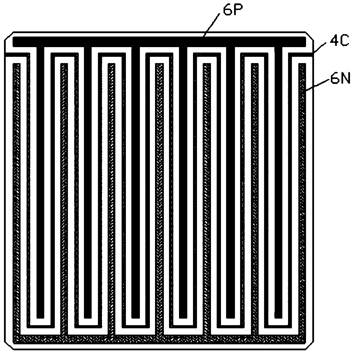
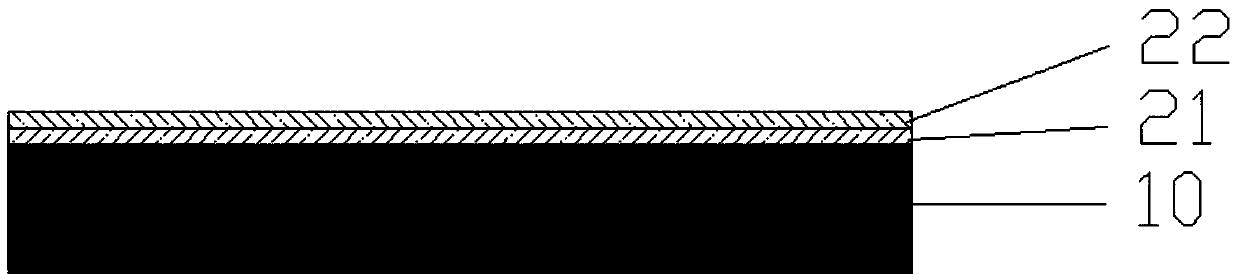
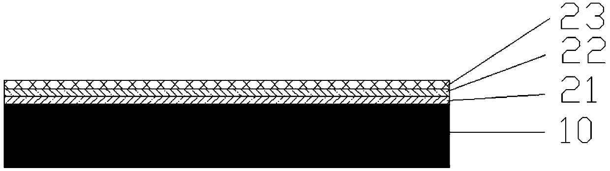
[0040] Such as figure 2 As shown, an N-type silicon wafer 10 that is textured and cleaned to form a textured surface is provided; a first intrinsic amorphous silicon layer 21 and an N-type amorphous silicon layer 22 are sequentially plated on the back side of the silicon wafer 10 to form a first semiconductor layer, The thickness of the first intrinsic amorphous silicon layer 21 and the N-type amorphous silicon layer 22 is 7nm, and the amorphous silicon film layer is deposited and formed by PECVD; as image 3 As shown, an insulating layer 23 is coated on the back side of the silicon wafer 10. The insulating layer 23 is silicon nitride with a thickness of 800nm. The insulating layer 23 is formed by PECVD deposition; Figure 4As shown, the insulating layer 23, the N-type amorphous silicon layer 22, and the first intrinsic amorphous silicon layer 21 in the corresponding area are etched and removed by printing etching paste on the local area of ​​the back side of the silicon wafe...

Embodiment 2

[0042] The difference from Example 1 is that, as Figure 13 As shown, the formation of the negative electrode lead-out groove 2N adopts the method of wet etching after printing the protective ink 3B on the back side of the silicon wafer 10. The protective ink 3B is an acid-resistant and not alkali-resistant ink. The curing temperature of the ink is 120°C, and the curing time is 10M. The wet etching solution is an HF solution containing a metal catalyst, and the protective ink 3B is removed by alkaline solution.

Embodiment 3

[0044] The difference from Example 1 is that, as Figure 14 As shown, the insulating groove 4C is formed by printing the protective ink 4B on the back side of the silicon wafer and then wet etching. The protective ink 4B is an acid-resistant and not alkali-resistant ink. The curing temperature of the ink is 120°C and the curing time is 10M. The wet etching solution is a mixed solution of hydrochloric acid and hydrogen peroxide, the etching time is 1 minute, and the protective ink 4B is removed by alkaline solution.

[0045] The present invention adopts the above-mentioned technical scheme, aiming at the characteristics of heterojunction thermal attenuation, the fabrication of the second semiconductor (i.e., the hole collector) occurs after the first semiconductor (i.e., the electron collector), so as to ensure that the thin film produced before has a higher High thermal stability and better quality, improve the quality of the produced products; by forming the insulating groove...


PUM

PropertyMeasurementUnit
thicknessaaaaaaaaaa
thicknessaaaaaaaaaa
thicknessaaaaaaaaaa

Abstract

The invention discloses a manufacturing method of a double-sided power generation back contact heterojunction solar cell. The manufacturing method comprises the following steps: providing an N-type orP-type silicon wafer which is textured and cleaned to form a textured surface; forming a first semiconductor layer and a second semiconductor layer on the back surface of the cell; forming a passivation film layer and a transparent anti-reflection layer on the front surface of the cell; depositing a transparent conductive film layer and a seed copper layer on the back surface of the cell; formingan insulating groove on the back surface of the battery by wet etching or printing etching paste; electroplating-resistant ink is printed, a copper grid line electrode is formed through electroplating, and the area occupied by the copper grid line electrode does not exceed 60% of the total area of the battery; and removing the electroplating-resistant ink and the copper seed layer outside the copper grid line electrode through a film-removing etching solution. According to the invention, the insulating groove is formed firstly and then the copper grid line electrode is formed, so that the copper grid line electrode and the insulating groove can independently adjust the required width, thereby realizing a relatively large light transmission area on the back surface, improving the power generation capacity of the back surface of the battery, realizing that the light transmission area on the back surface reaches 40%-90%, realizing double-sided power generation and greatly improving the power generation capacity of the module.

Description

technical field [0001] The invention relates to the technical field of solar cells, in particular to a method for manufacturing a back-contact heterojunction solar cell with double-sided power generation. Background technique [0002] A solar cell is a semiconductor device that can convert solar energy into electrical energy. Under the condition of light, a photogenerated current will be generated inside the solar cell, and the electrical energy will be output through the electrodes. In recent years, the production technology of solar cells has been continuously improved, the production cost has been continuously reduced, and the conversion efficiency has been continuously improved. The application of solar cell power generation has become increasingly widespread and has become an important energy source for power supply. [0003] High-efficiency solar cells are the trend of the future industry, because high-efficiency solar cells not only increase the power generation watta...

Claims


Application Information

Patent Timeline
Patent Type & Authority Applications(China)
IPC IPC(8): H01L31/0224H01L31/074H01L31/20
CPCH01L31/022441H01L31/074H01L31/202H01L31/208Y02E10/50Y02P70/50
Inventor 张超华谢志刚林振鹏白述铭林锦山王树林林朝晖
Owner GOLD STONE (FUJIAN) ENERGY CO LTD
Why Eureka
Try Eureka