Graphical single crystal film preparing method, graphical single crystal film and harmonic oscillator

A single crystal thin film and patterning technology, applied in the field of patterned single crystal thin film preparation, patterned single crystal thin film and resonators, can solve the problem of high preparation conditions, difficult to control bonding pressure, and easy damage to the device single crystal thin film area. and other problems, to avoid incompatibility and relieve stress accumulation.

Active Publication Date: 2020-04-03
CHIMEMS MICROELECTRONICS CO LTD
View PDF6 Cites 10 Cited by
  • Summary
  • Abstract
  • Description
  • Claims
  • Application Information

AI Technical Summary

Problems solved by technology

[0007] The object of the present invention is to provide a method for preparing a patterned single crystal thin film, a patterned single crystal thin film and a resonator, through the method for preparing a patterned single crystal thin film to solve the problem of high requirements for preparation conditions in the prior art: the whole chip Wafer bonding peeling, the bonding pressure is not easy to control, and the stress accumulation is too large, which is easy to damage the single crystal thin film area required by the device

Method used


Image

  • Graphical single crystal film preparing method, graphical single crystal film and harmonic oscillator
  • Graphical single crystal film preparing method, graphical single crystal film and harmonic oscillator
  • Graphical single crystal film preparing method, graphical single crystal film and harmonic oscillator

Examples


preparation example Construction

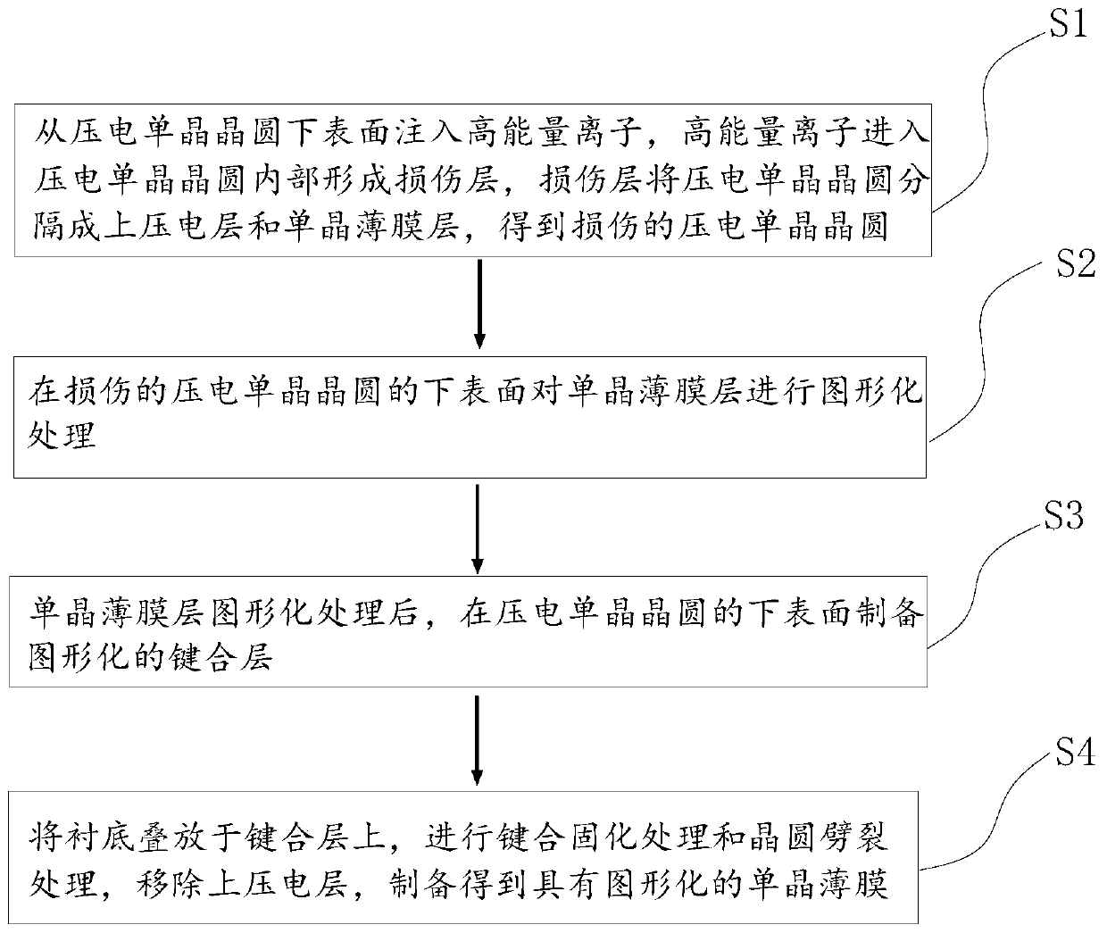
[0038] A method for preparing a patterned single crystal thin film, comprising the steps of:

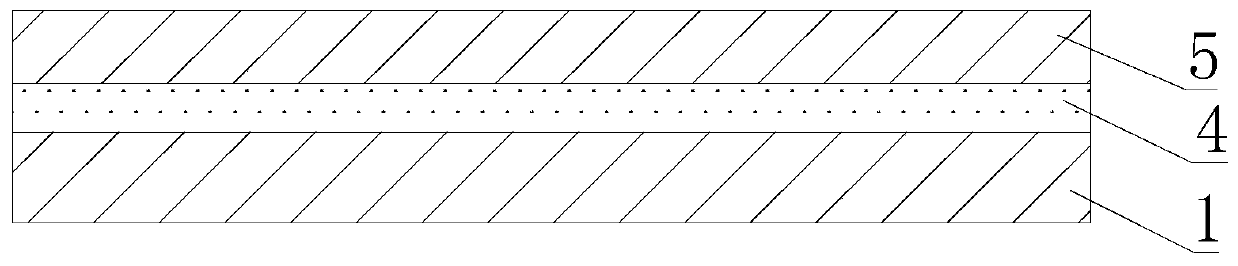
[0039] S1) High-energy ions A are injected from the lower surface of the piezoelectric single-crystal wafer, and the high-energy ions A enter the interior of the piezoelectric single-crystal wafer to form a damaged layer 4, and the damaged layer 4 separates the piezoelectric single-crystal wafer into an upper piezoelectric layer 5 and single crystal thin film layer 1 to obtain a damaged piezoelectric single crystal wafer;

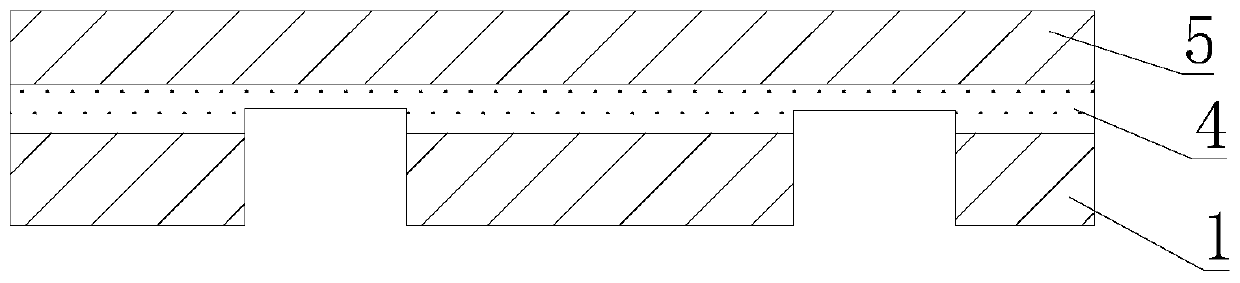
[0040] S2) patterning the single crystal thin film layer 1 on the lower surface of the damaged piezoelectric single crystal wafer;

[0041] S3) After patterning the single crystal thin film layer 1, prepare a patterned bonding layer 2 on the lower surface of the piezoelectric single crystal wafer;

[0042] S4) Lay the substrate 3 on the bonding layer, perform bonding curing treatment and wafer splitting treatment, remove the upper piezoelectric layer, and prepare...

Embodiment 1

[0058] This embodiment proposes a preparation process of a patterned lithium niobate single crystal thin film, specifically:

[0059] 1) A lithium niobate piezoelectric single crystal wafer is selected, and positive monovalent helium ions (He + ), the implantation depth is 0.3 μm; a damaged layer is formed inside the lithium niobate piezoelectric single crystal wafer, and the damaged layer divides the lithium niobate piezoelectric single crystal wafer into an upper lithium niobate piezoelectric layer and a lithium niobate single crystal wafer. crystal thin film layer;

[0060] 2) Coating photoresist on the lower surface of the damaged lithium niobate piezoelectric single crystal wafer, exposing the photoresist with a patterned mask plate, and developing with a developing solution to obtain a patterned photoresist mask film, performing ion beam sputtering etching on the lithium niobate single crystal thin film layer with a patterned photoresist mask, the etching depth is great...

Embodiment 2

[0067] This embodiment proposes a preparation process of a patterned lithium tantalate single crystal thin film, specifically:

[0068] 1) A lithium tantalate piezoelectric single crystal wafer is selected, and positive monovalent hydrogen ions (H + ), the implantation depth is 2 μm; a damage layer is formed inside the lithium tantalate piezoelectric single crystal wafer, and the damage layer divides the lithium tantalate piezoelectric single crystal wafer into an upper lithium tantalate piezoelectric layer and a lithium tantalate single crystal film layer;

[0069] 2) Coating photoresist on the lower surface of the damaged lithium tantalate piezoelectric single crystal wafer, exposing the photoresist with a patterned mask plate, developing with a developer, and obtaining a patterned photoresist mask Reactive ion etching (RIE) is carried out to the lithium tantalate single crystal film layer with a patterned photoresist mask, the depth of etching is greater than the thickness...


PUM


Abstract

The invention relates to the technical field of single crystal film preparing, in particular to a graphical single crystal film preparing method, a graphical single crystal film and a harmonic oscillator. The method comprises the following steps that high-energy ions are injected from the lower surface of a piezoelectric single crystal wafer, a damage layer is formed, and a damaged piezoelectric single crystal wafer is obtained; on the lower surface of the damaged piezoelectric single crystal wafer, a single crystal film layer is subjected to graphical processing; a graphical bonding layer isprepared again; and a substrate is stacked on the bonding layer, bonding curing treatment and wafer fracturing treatment are carried out, an upper piezoelectric layer is removed, and the graphical single crystal film is prepared. Through the graphical single crystal film preparing method, the technical problems that in the prior art, when a whole wafer is subjected to bonding stripping, bonding pressure is not prone to control, stress stacking is too large, and the single crystal film area needed by a device is easily damaged can be solved.

Description

technical field [0001] The invention relates to the technical field of single crystal thin film preparation, in particular to a method for preparing a patterned single crystal thin film, a patterned single crystal thin film and a resonator. Background technique [0002] In order to meet the high integration of wireless mobile communications, the demand for single-crystal thin films in the MEMS manufacturing process (Microfabrication Process) continues to increase. Under the condition that the molecular beam derivatization length cannot meet the growth of single-crystal thin films with a fixed crystal orientation, the ion Infused peel technology. [0003] However, the combination of ion implantation stripping technology and bonding technology requires full-area bonding, wafer splitting, and single-crystal thin films in sequence in the device manufacturing process, and then the single-crystal thin films are patterned using photolithography and etching processes. processing. ...

Claims


Application Information

Patent Timeline
Patent Type & Authority Applications(China)
IPC IPC(8): C23C14/48C23C14/58H03H9/17
CPCC23C14/48C23C14/588H03H9/171
Inventor 罗文博简珂吴传贵帅垚
Owner CHIMEMS MICROELECTRONICS CO LTD
Why Eureka
Try Eureka