Single-chip white light emitting diode and preparation method thereof

A single-chip, white light technology, applied in the direction of electrical components, circuits, semiconductor devices, etc., can solve the problems of reduced radiation luminous efficiency, high cost, high color rendering index, etc., to achieve color rendering performance, avoid etching damage, ultra-high The effect of color rendering performance

Active Publication Date: 2020-04-21
XIAMEN UNIV
View PDF11 Cites 7 Cited by
  • Summary
  • Abstract
  • Description
  • Claims
  • Application Information

AI Technical Summary

Problems solved by technology

At present, there are two main methods to realize white LEDs: one is to use blue light chips to excite yellow light phosphors, or to use ultraviolet light chips to excite red, green and blue light phosphors to obtain white light LEDs; the advantages are mature technology, relatively simple preparation, and low price. Relatively cheap, it is the mainstream method used in the current semiconductor lighting industry. The disadvantage is that the aging of phosphor powder and packaging materials will reduce the life, stability and color rendering index of white LEDs.
The second is to synthesize white light through multi-chip combination of red, green and blue (RGB) three primary colors; its advantage is that the color rendering index is high, and the light color can be easily controlled by independently adjusting the current of each color chip. The disadvantage is that the control circuit is relatively complicated and the cost is high.
However, during the preparation of nanopores, the etching technique will cause great damage to the active region of the quantum well, resulting in a decrease in its radiative luminous efficiency.

Method used


Image

  • Single-chip white light emitting diode and preparation method thereof
  • Single-chip white light emitting diode and preparation method thereof

Examples


Embodiment Construction

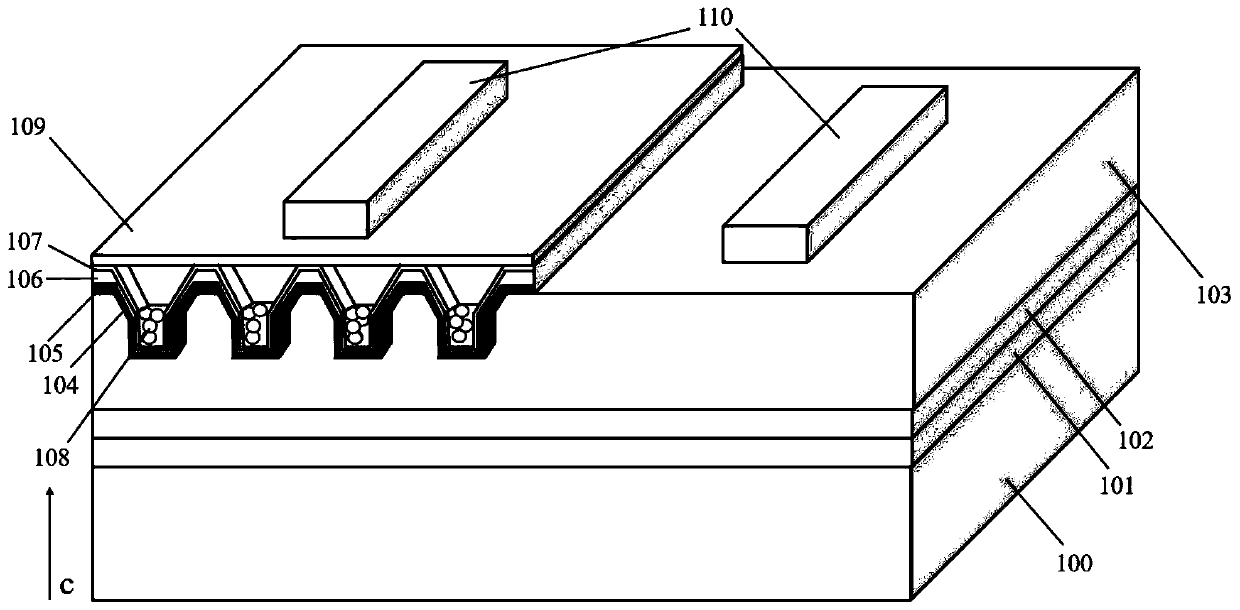
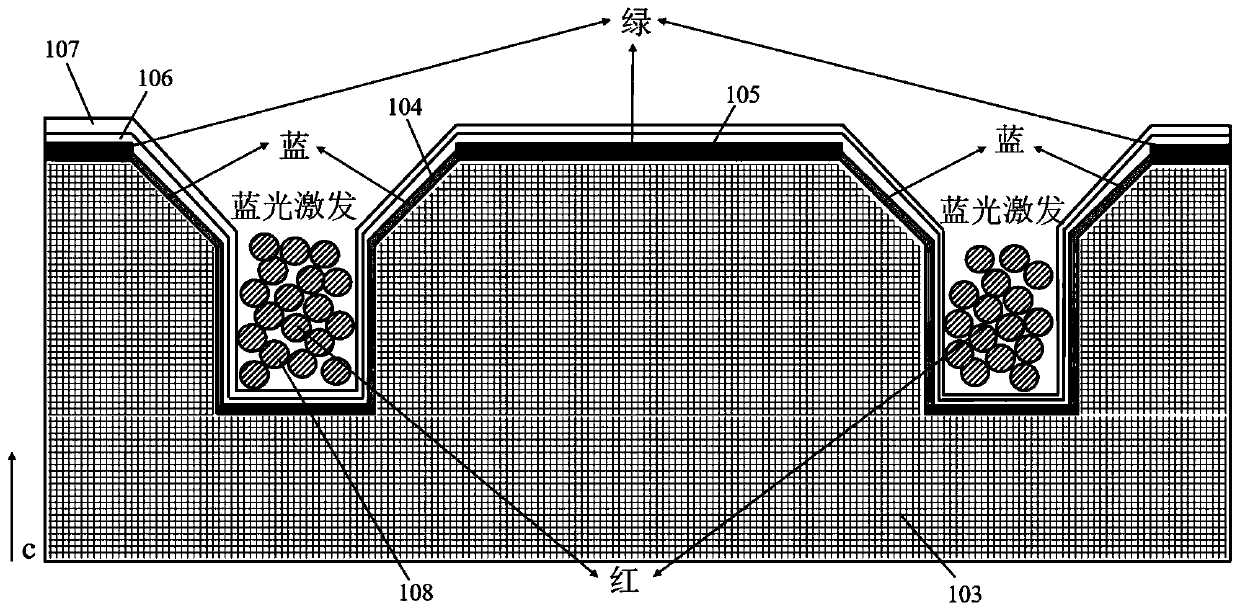
[0029] The present invention will be further described below through specific embodiments. The drawings of the present invention are only schematic diagrams for easier understanding of the present invention, and their specific proportions can be adjusted according to design requirements. The upper and lower relationship of the relative components in the figures described herein should be understood by those skilled in the art to refer to the relative positions of the components. Correspondingly, the upper side of the component is the front and the lower side is the back for easy understanding, so all The same components can be turned over to present, all of which should belong to the scope disclosed in this specification.

[0030] The structure of a single-chip white light LED prepared by the present invention is as follows: figure 1 As shown, it mainly includes a substrate 100, a buffer layer 101, a non-doped GaN layer 102, a patterned n-type semiconductor layer 103, a quant...


PUM

PropertyMeasurementUnit
thicknessaaaaaaaaaa
thicknessaaaaaaaaaa
thicknessaaaaaaaaaa

Abstract

The invention discloses a single-chip white light emitting diode, which comprises a substrate, a buffer layer, a non-doped GaN layer, a patterned n-type GaN layer, a multi-quantum well active layer, an electron blocking layer, a p-type GaN layer, a red light wavelength conversion material, a current expansion layer, and n-type and p-type ohmic contact electrodes, wherein the n-type GaN layer is etched through a dry etching technology and a wet etching technology to form a hexagonal hole array with a semi-polar surface, a non-polar surface and a polar surface, the InGaN multi-quantum well active layer, the electron blocking layer and the p-type GaN layer are epitaxially grown on the patterned n-type GaN layer, and a wide spectrum from blue light to a yellow-green light waveband is emitted;and the hexagonal holes are filled with the red light wavelength conversion material, and a red light spectrum is excited by blue / green light emitted by the quantum well active region, so that a fullspectrum is formed, and the single-chip white light emitting diode with a high color rendering index is obtained.

Description

technical field [0001] The invention belongs to the technical field of semiconductor optoelectronic devices, and relates to a gallium nitride-based phosphor-free single-chip white light emitting diode. Background technique [0002] Light-emitting diodes (LEDs), especially white LEDs, have played an increasingly important role in lighting, display and other fields. At present, there are two main methods to realize white LEDs: one is to use blue light chips to excite yellow light phosphors, or to use ultraviolet light chips to excite red, green and blue light phosphors to obtain white light LEDs; the advantages are mature technology, relatively simple preparation, and low price. It is relatively cheap and is currently the mainstream method used in the semiconductor lighting industry. The disadvantage is that the aging of phosphors and packaging materials will reduce the life, stability and color rendering index of white LEDs. The second is to synthesize white light through mu...

Claims


Application Information

Patent Timeline
Patent Type & Authority Applications(China)
IPC IPC(8): H01L33/32H01L33/24H01L33/06H01L33/00H01L33/14H01L33/12
CPCH01L33/0075H01L33/06H01L33/12H01L33/14H01L33/24H01L33/32
Inventor 李金钗王传家陈航洋卢诗强黄凯康俊勇
Owner XIAMEN UNIV
Why Eureka
Try Eureka