Package substrate distributed antenna

A distributed antenna and packaging substrate technology, applied in the direction of the connection of the antenna grounding switch structure and the structure of the radiating element, can solve the problems of limited application range of the antenna, difficult chip packaging, limited gain, etc., and achieve multiple design freedom and flexibility. performance, reducing design cycle and cost, and reducing loss

Active Publication Date: 2020-04-21
SOUTH CHINA UNIV OF TECH
View PDF9 Cites 3 Cited by
  • Summary
  • Abstract
  • Description
  • Claims
  • Application Information

AI Technical Summary

Problems solved by technology

[0006] 1. Encapsulated antenna: Due to the limitation of interconnection loss, it is difficult to apply to the middle and high frequency bands of millimeter waves;
[0007] 2. On-chip antenna: If the high-resistance silicon lens solution is used, the substrate surface wave loss can be avoided and high gain can be achieved, but the lens is large in size and high in profile, which also makes it difficult to package the chip; if other solutions are used, it is limited by the on-chip antenna Aperture and loss, the gain will be very limited;
[0008] 3. Chip-packaged distributed antenna: limited by the size of the chip and package, it is only applicable to the high frequency band of millimeter wave and the terahertz frequency band, and cannot be applied to the low frequency band of millimeter wave (such as the 5G millimeter wave frequency band);
If the application changes, the antenna needs to be redesigned, which limits the application range of the antenna

Method used


Image

  • Package substrate distributed antenna
  • Package substrate distributed antenna
  • Package substrate distributed antenna

Examples


Embodiment Construction

[0039] The present invention will be further described in detail through specific embodiments below, but the embodiments of the present invention are not limited thereto.

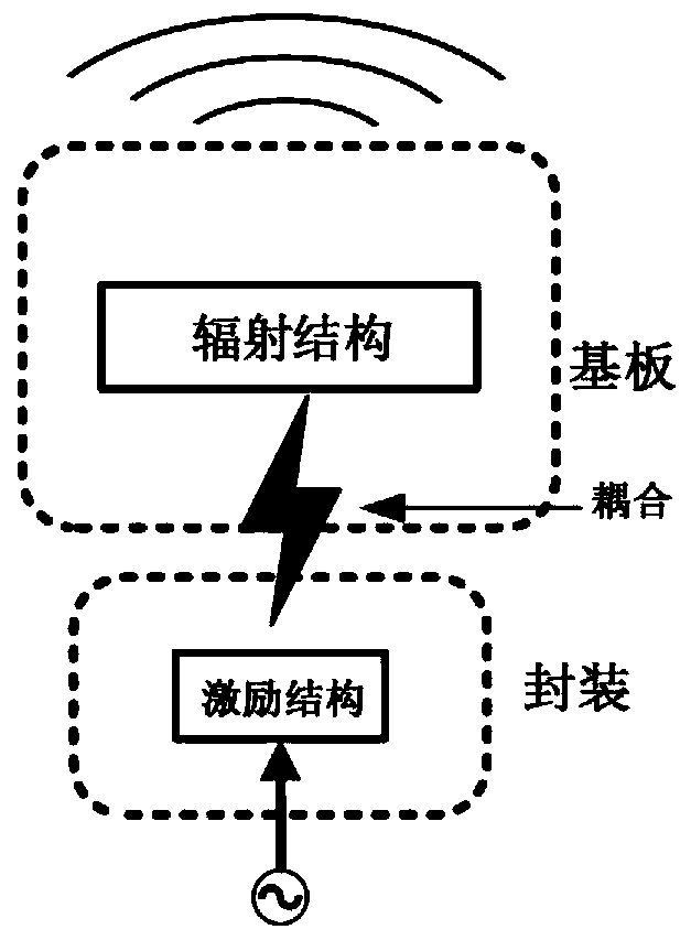
[0040] A packaged substrate distributed antenna, including two basic parts, the first basic part is an excitation structure, located on the package; the second basic part is a radiation structure, located on the substrate; the package is welded to the substrate to obtain the overall structure of the antenna, The two basic parts are interconnected through coupling, and the schematic diagram of its structure is shown in figure 1 shown.

[0041] According to the idea of ​​the present invention, a specific design example of a packaged substrate distributed antenna working in the 5G millimeter wave frequency band (24.25-29.5GHz) is given below.

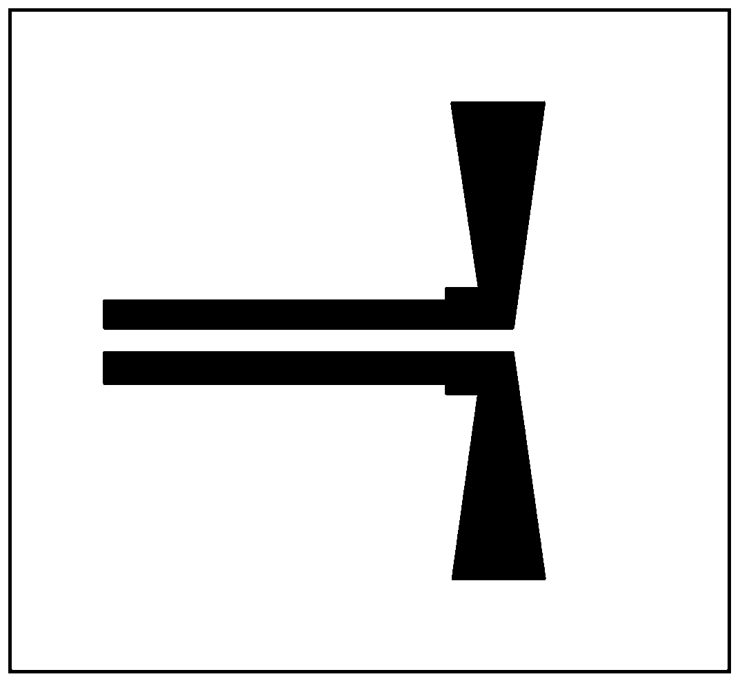
[0042] (1) The excitation structure located in the package

[0043] The excitation structure uses a fully differential input dipole antenna, such as figure 2 shown....


PUM


Abstract

The invention belongs to the field of antennas of electronic communication technology, and relates to a package substrate distributed antenna. The antenna structure is distributed and designed on a package and a substrate, low-loss interconnection of electromagnetic signals from the package to the substrate is realized through coupling inside the antenna instead of conductor connection, and the package and the substrate are interconnected through electromagnetic coupling. With application of the radiation structure integrated on the substrate, electromagnetic waves coupled by the package are radiated in a specific mode. The package substrate distributed antenna is multiplexed by changing the substrate, and the multiplexing of the package substrate distributed antenna is realized by changing the radiation structure on the substrate without changing the package. The internal interconnection loss of the antenna is reduced, the limitation of the working frequency band of a chip package distributed antenna is solved, the realization of a millimeter wave low-frequency-band distributed antenna becomes possible, more design freedom degrees and flexibility are brought to the design of the millimeter wave antenna, the design period and cost of the millimeter wave integrated antenna are reduced, and the multiplexing of the package design is realized.

Description

technical field [0001] The invention belongs to the antenna field of electronic communication technology, and relates to a packaged substrate distributed antenna. Background technique [0002] Antennas are an integral part of any wireless system and come in both discrete and integrated forms. Split antennas are the most common form of traditional wireless systems. In the millimeter-wave frequency band, the integration of wireless systems based on separate antennas is low, and the front-end and antennas need to be interconnected multiple times, causing large losses and degrading system performance. In recent years, with the advancement of technology, high integration has become the development trend of wireless systems, and integrated antennas just follow this trend. It overcomes the problems of separate antennas and provides a good solution for system-level wireless chips. The antenna solution is very suitable for applications in the mmWave frequency band. Current integra...

Claims


Application Information

Patent Timeline
Patent Type & Authority Applications(China)
IPC IPC(8): H01Q1/36H01Q1/38H01Q1/50
CPCH01Q1/36H01Q1/38H01Q1/50
Inventor 冯群倚薛泉廖绍伟张文海
Owner SOUTH CHINA UNIV OF TECH
Why Eureka
Try Eureka