Composite single crystal piezoelectric substrate film and preparation method thereof
A single crystal and substrate technology, which is applied in the manufacture of circuits, electrical components, semiconductors/solid-state devices, etc., can solve the problems of difficult and complete separation of thin films, low yield of single crystal thin films, and easy breakage of substrates, etc. Thermal separation, fast and complete separation, satisfying the effect of large-scale industrial production
- Summary
- Abstract
- Description
- Claims
- Application Information
AI Technical Summary
Problems solved by technology
Method used
Image

Examples
preparation example Construction
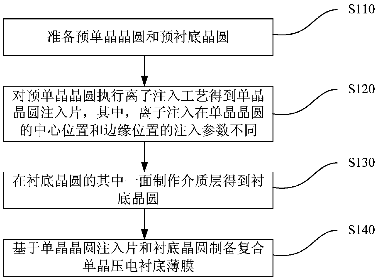
[0035] A method for preparing a composite single crystal piezoelectric substrate film, such as figure 1 shown, including the following steps:
[0036] In step S110, a pre-single crystal wafer and a pre-substrate wafer are prepared;
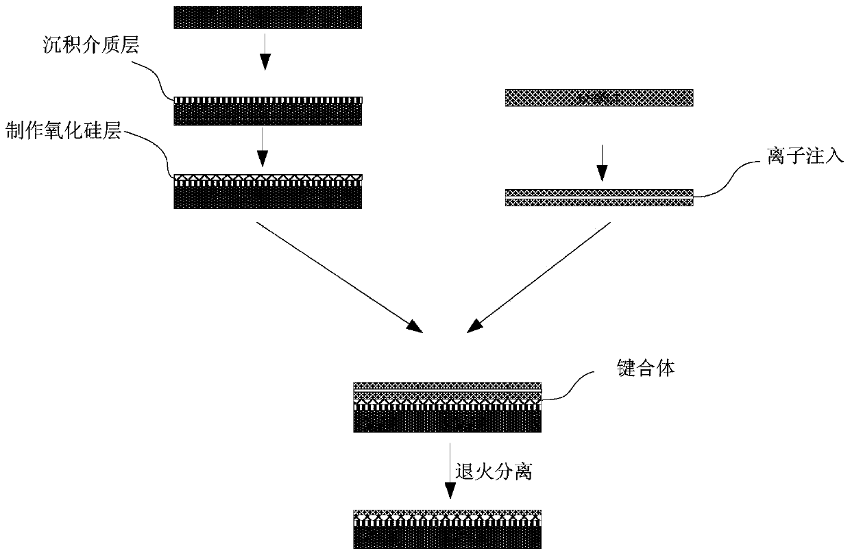
[0037] The pre-single-crystal wafer is a semi-finished product obtained by polishing and cleaning the single-crystal wafer. Similarly, the pre-substrate wafer is also a semi-finished product with a smooth surface after polishing and cleaning. Among them, chemical mechanical polishing is used in the polishing process, and semiconductor RCA is used in the cleaning process to obtain a crystallized surface.
[0038] In step S120, an ion implantation process is performed on the pre-single-crystal wafer to obtain a single-crystal wafer implantation sheet, wherein the implantation parameters of the ion implantation are different at the center position and the edge position of the single-crystal wafer;
Embodiment 1
[0075] A method for preparing a composite single crystal piezoelectric substrate film, comprising the following steps:
[0076] ①Provide a 200μm silicon wafer and a 200μm lithium niobate wafer, respectively fix the silicon wafer or lithium niobate on the porous ceramic chuck of the polishing equipment, perform chemical mechanical polishing to obtain a smooth surface, and then polish the two wafers Perform semiconductor RCA cleaning to obtain a clean surface;
[0077] ②The lithium niobate wafer processed in step ① is implanted with He by ion implantation + , so that the lithium niobate wafer is sequentially divided into a separation layer, an implanted layer and a residual layer from the implanted surface, and the implanted ions are distributed in the implanted layer to obtain a single crystal wafer implanted sheet;
[0078] He was implanted by ion implantation + , adjust the implant dose parameters at the center and edge of the lithium niobate wafer, specifically:
[0079] ...
Embodiment 2
[0090] A method for preparing a composite single crystal piezoelectric substrate film, comprising the following steps:
[0091] ①Provide a 500μm silicon carbide wafer and a 500μm lithium tantalate wafer, respectively fix the silicon carbide wafer or lithium tantalate wafer on the porous ceramic chuck of the polishing equipment, perform chemical mechanical polishing to obtain a smooth surface, and then The two wafers are cleaned by semiconductor RCA to obtain a clean surface;
[0092] ②The lithium tantalate wafer processed in step ① was implanted with H + , the lithium tantalate wafer is sequentially divided into a separation layer, an implanted layer and a residual layer from the implanted surface, and the implanted ions are distributed in the implanted layer to obtain a single crystal wafer implanted sheet;
[0093] H was implanted by ion implantation + , adjust the temperature parameters at the center and edge of the lithium tantalate wafer, specifically:
[0094] The tem...
PUM
| Property | Measurement | Unit |
|---|---|---|
| thickness | aaaaa | aaaaa |
| thickness | aaaaa | aaaaa |
| thickness | aaaaa | aaaaa |
Abstract
Description
Claims
Application Information
 - R&D
- Intellectual Property
- Life Sciences
- Materials
- Tech Scout
- Unparalleled Data Quality
- Higher Quality Content
- 60% Fewer Hallucinations
Browse by: Latest US Patents, China's latest patents, Technical Efficacy Thesaurus, Application Domain, Technology Topic, Popular Technical Reports.
© 2025 PatSnap. All rights reserved.Legal|Privacy policy|Modern Slavery Act Transparency Statement|Sitemap|About US| Contact US: help@patsnap.com