
Metal-clad laminate, circuit board, multilayer circuit board, and method for producing same

A technology of circuit substrates and laminated boards, applied in the direction of multilayer circuit manufacturing, printed circuit manufacturing, circuit substrate materials, etc., can solve the problems of high-frequency signal transmission application possibilities that have not been studied, and achieve high-density integration and durability Excellent thermal performance and good interlayer connection effect

Pending Publication Date: 2020-05-08
NIPPON STEEL CHEMICALL &MATERIAL CO LTD
View PDF2 Cites 0 Cited by
  • Summary
  • Abstract
  • Description
  • Claims
  • Application Information

AI Technical Summary

Problems solved by technology

However, in Patent Document 2, the possibility of application to high-frequency signal transmission is not studied.

Method used


Image

  • Metal-clad laminate, circuit board, multilayer circuit board, and method for producing same
  • Metal-clad laminate, circuit board, multilayer circuit board, and method for producing same
  • Metal-clad laminate, circuit board, multilayer circuit board, and method for producing same

Examples


no. 1 approach >

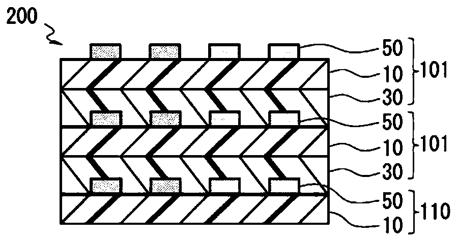
[0179] image 3 It is a cross-sectional view in the stacking direction showing the structure of the multilayer circuit board 200 according to the first embodiment of the present invention. The multilayer circuit board 200 of the first embodiment has a structure in which a plurality of circuit boards 101 and an arbitrary circuit board 110 are stacked in the same direction.

[0180] That is, since image 3 The upper side of the first circuit board 101 faces the lower side, and the adhesive layer 30 of the first circuit board 101 is in contact and laminated so as to cover the conductor circuit layer 50 of the second circuit board 101. Furthermore, the adhesive layer 30 of the second circuit board 101 The conductor circuit layer 50 of the arbitrary circuit board 110 which does not have the adhesive layer 30 may be contact|connected and laminated so that it may cover. Here, the structure or material of any circuit substrate 110 is not limited. For example, the conductive circuit layer...

no. 2 approach >

[0187] Figure 5 It is a cross-sectional view in the stacking direction showing the structure of the multilayer circuit board 201 according to the second embodiment of the present invention. In the multilayer circuit board 201 of the second embodiment, a structure in which a pair of circuit boards 101 are bonded such that these adhesive layers 30 face each other is set as one circuit board unit 102, and includes at least one The circuit board unit 102.

[0188] That is, since Figure 5 In the upper part facing downward, the first metal-clad laminate 100, the circuit board unit 102, and the second metal-clad laminate 100 (wherein the opposite direction to the first metal-clad laminate 100) are arranged in this order, and The circuit board unit 102 is sandwiched between the adhesive layers 30 of the two metal-clad laminates 100 and laminated. The adhesive layer 30 of the first metal-clad laminate 100 is laminated so as to be in contact with the conductor circuit layer 50 on the si...

Embodiment

[0195] Examples are shown below, and the features of the present invention will be described in more detail. However, the scope of the present invention is not limited to the examples. In addition, in the following examples, unless otherwise specified, various measurements and evaluations are based on the following.

[0196] [Measurement of dimensional change rate]

[0197] The measurement of the dimensional change rate is performed in the following procedure. First, a 150 mm square test piece was used to expose and develop the dry film resist at intervals of 100 mm, thereby forming a target for position measurement. In an environment with a temperature of 2322°C and a relative humidity of 5025%, the size before etching (normal) is measured, and thereafter, copper other than the target of the test piece is removed by etching (liquid temperature of 40°C or less, time within 10 minutes). After standing for 2424 hours in an environment with a temperature of 2322°C and a relative hu...


PUM

PropertyMeasurementUnit
elastic modulusaaaaaaaaaa
glass transition temperatureaaaaaaaaaa

Abstract

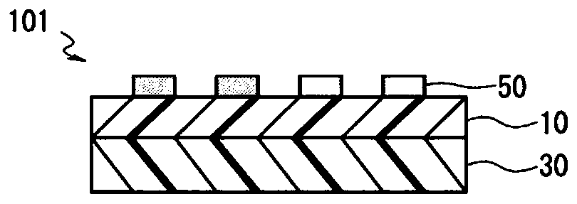
The invention provides a metal-clad laminate, a circuit board, a multilayer circuit board, and a method for producing the same. To provide a multilayer circuit board having an adhesive layer excellentin dimensional stability of a conductor circuit and capable of reducing transmission loss even in transmission of a high frequency signal. The circuit board 101 includes an insulating resin layer 10,a conductor circuit layer 10 laminated on one surface of the insulating resin layer 10, and an adhesive layer 30 laminated on the other surface of the insulating resin layer 50. The multilayer circuit board 200 is manufactured by disposing an adhesive layer 30 of a first circuit board 101 so as to face a conductor circuit layer 50 of an arbitrary circuit board 110 which is opposed to a conductorcircuit layer 50 of a 2 circuit board 101 and an adhesive layer 30 of a 2 circuit board 101 without an adhesive layer 30, and press-bonding them together.

Description

Technical field [0001] The present invention relates to a metal-clad laminate, a circuit substrate, and a multilayer circuit substrate with conductor circuit layers laminated in multiple layers and a manufacturing method thereof. Background technique [0002] In recent years, with the advancement of high-density and high-functionality of electronic equipment, circuit board materials with further dimensional stability or excellent high-frequency characteristics are required. In particular, low dielectric constant and low dielectric loss are important for the characteristics of organic interlayer insulating materials required for high-speed signal processing. In order to cope with the increase in high frequency, a multilayer wiring board in which a liquid crystal polymer (LCP) characterized by a low dielectric constant and a low dielectric loss tangent is used as a dielectric layer has been proposed (for example, Patent Document 1). A multilayer wiring board in which a liquid crys...

Claims


Application Information

Patent Timeline
Patent Type & Authority Applications(China)
IPC IPC(8): H05K1/03H05K3/46C09J163/00C09J133/04C09J161/04C09J11/04C09J11/08C09J179/08
CPCH05K1/036H05K3/4626C09J163/00C09J11/04C09J11/08C09J179/08C08L2205/03C08L33/04C08L61/04C08K3/013B32B15/08B32B7/12C09J179/04H05K1/0313H05K3/4655B32B2457/08H05K2201/0154C09J2479/08
Inventor 铃木智之须藤芳树安藤智典
Owner NIPPON STEEL CHEMICALL &MATERIAL CO LTD
Learn More