Silicon wafer
A technology for silicon wafers and semiconductors, applied in crystal growth, single crystal growth, single crystal growth, etc., can solve the problems of increased bending of silicon wafers, increased film stress, etc., and achieve the effect of reducing wafer bending and improving suppression
- Summary
- Abstract
- Description
- Claims
- Application Information
AI Technical Summary
Problems solved by technology
Method used
Image

Examples
Embodiment 1)
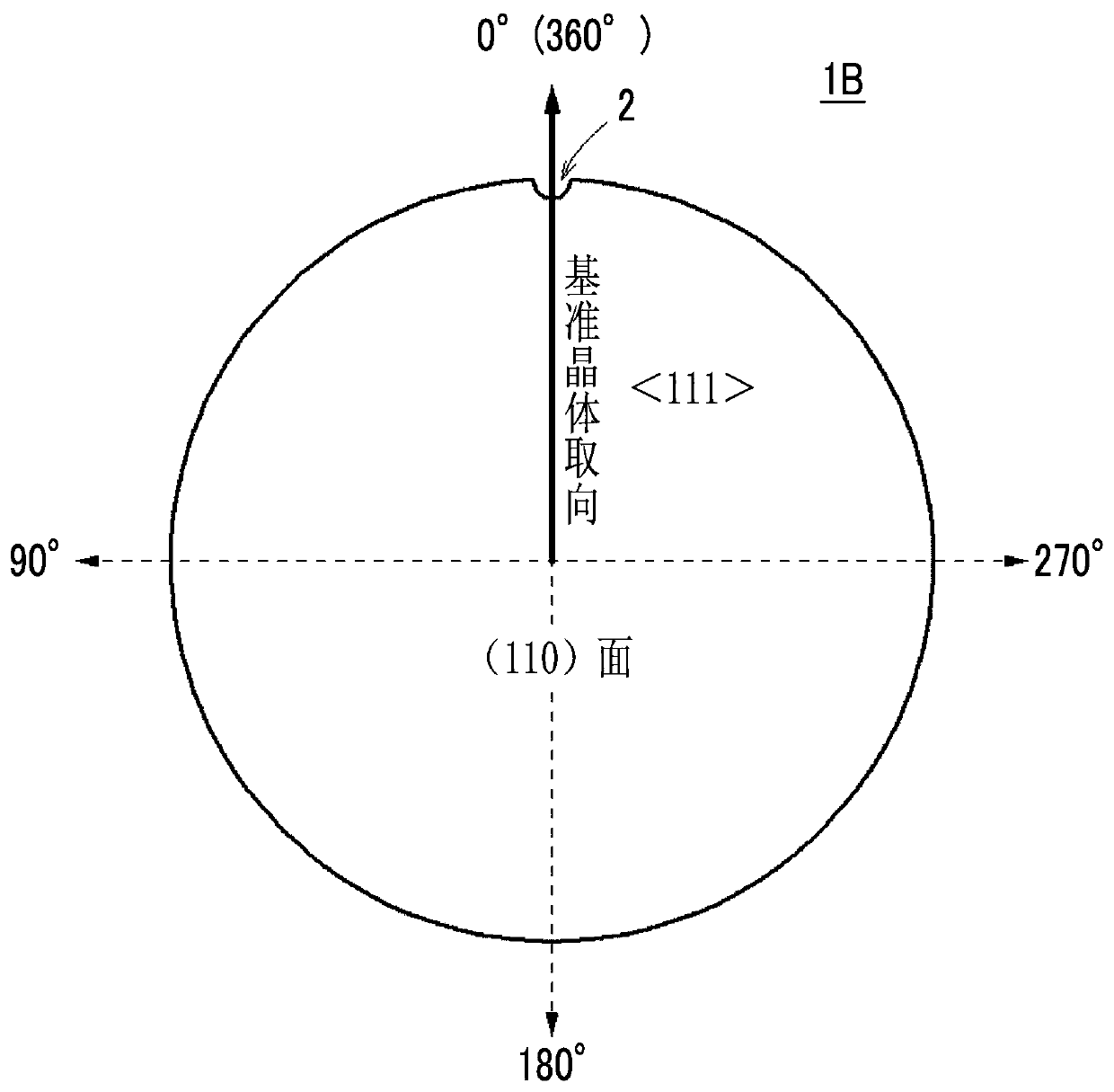
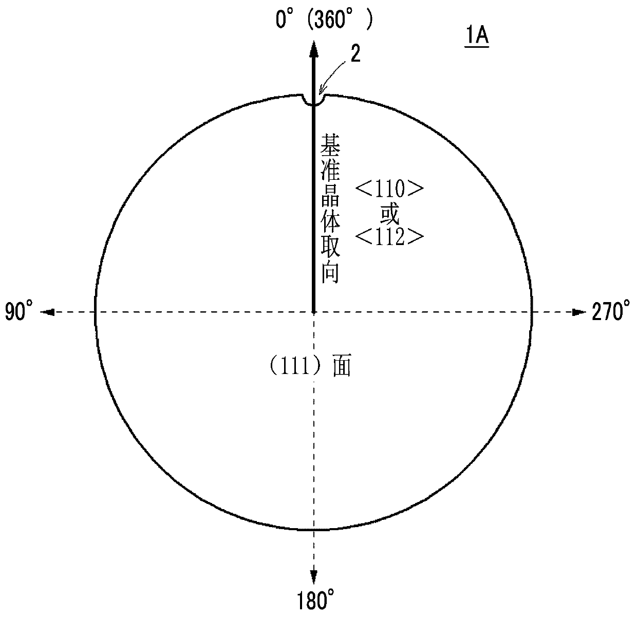
[0054] Samples #1 to #16 of silicon wafers having different plane orientations and notch orientations were prepared. Each wafer was grown by the CZ method and had a diameter of 300 mm and a thickness of 775 μm. There are three plane orientations of the wafer sample: (100), (110), and (111). The notch orientations of the plane-oriented (100) wafer are and . The notch orientation of the plane-oriented (110) wafer is There are two types of orientations: and , and two types of notch orientations in the plane-oriented (111) wafer: and . The deviation of the plane orientation and the notch orientation of the wafer used was within ±1 degree.
[0055] Next, the oxygen concentration of each wafer was measured. In addition, all oxygen concentrations are values measured by Fourier transform infrared spectrophotometry (FT-IR) standardized by ASTM F121, 1979.
[0056] Next, when a silicon oxide film with a thickness of 2 μm was formed on the main surfaces of these wafer samples #1 ...
Embodiment 2)
[0064] In the same manner as in Example 1, samples #17 to #31 of silicon wafers having different plane orientations and notch orientations were prepared, and the oxygen concentrations of these wafers were measured.
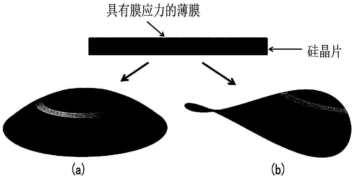
[0065] Next, after forming a silicon oxide film with a thickness of 1 μm on the main surfaces of these wafer samples #17 to #31 by a CVD process, a part of etching was performed using a mask, and then a silicon nitride film with a thickness of 0.7 μm was formed by a CVD process, and then a silicon nitride film was formed using a mask to The mold is partially etched to produce a Figure 5 The shape of the membrane is shown. For example, in the case of the (100) wafer of sample #17, the silicon oxide film is a rectangular pattern elongated in the orientation, and the silicon nitride film is elongated in a direction perpendicular to the long side direction of the silicon oxide film. rectangle pattern. With this composite pattern, anisotropic film stress is generat...
PUM
| Property | Measurement | Unit |
|---|---|---|
| thickness | aaaaa | aaaaa |
| thickness | aaaaa | aaaaa |
| thickness | aaaaa | aaaaa |
Abstract
Description
Claims
Application Information
 - R&D Engineer
- R&D Manager
- IP Professional
- Industry Leading Data Capabilities
- Powerful AI technology
- Patent DNA Extraction
Browse by: Latest US Patents, China's latest patents, Technical Efficacy Thesaurus, Application Domain, Technology Topic.
© 2024 PatSnap. All rights reserved.Legal|Privacy policy|Modern Slavery Act Transparency Statement|Sitemap