Preparation method of surface-enhanced Raman substrate with layered micro/nano structure

A nanostructured, surface-enhanced technology, applied in Raman scattering, material analysis, material excitation analysis, etc., to achieve the effect of economical preparation process, broad application prospects, and good wettability

Active Publication Date: 2020-05-19
SOUTHWEAT UNIV OF SCI & TECH
View PDF8 Cites 12 Cited by
  • Summary
  • Abstract
  • Description
  • Claims
  • Application Information

AI Technical Summary

Problems solved by technology

[0003] However, although considerable efforts have been invested in developing various SERS substrates with hierarchical micro / nanostructures to obtain sufficient sensitivity while maintaining appropriate superhydrophobicity, it is still difficult to integrate superhydrophobicity and Combining hotspots with plasmonic nanostructures remains a challenge

Method used


Image

  • Preparation method of surface-enhanced Raman substrate with layered micro/nano structure
  • Preparation method of surface-enhanced Raman substrate with layered micro/nano structure
  • Preparation method of surface-enhanced Raman substrate with layered micro/nano structure

Examples


preparation example Construction

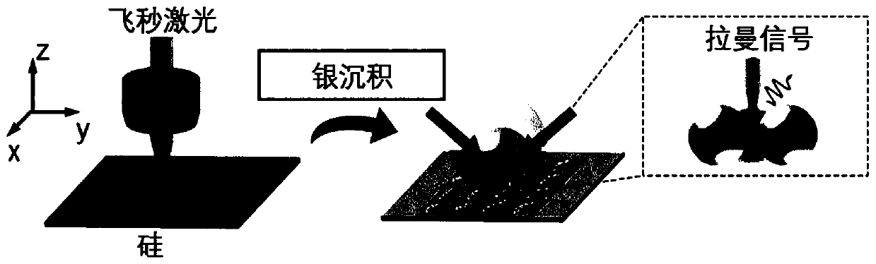
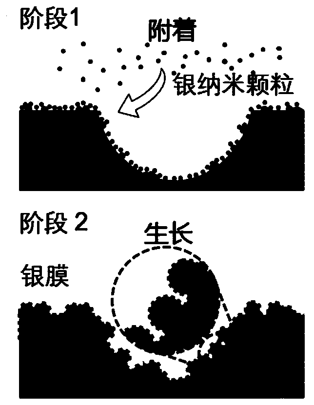
[0040] A surface-enhanced Raman substrate with a layered micro / nano structure can be obtained through the preparation method of this exemplary embodiment. The surface-enhanced Raman substrate is composed of a semiconductor substrate with a micropit array and a silver thin film with a thickness of 40-300 nm deposited on the micropit array of the semiconductor substrate, wherein the micropit array is formed by nanosecond It is formed by irradiating a semiconductor substrate with laser pulses up to femtoseconds, the diameter of each micro-pit in the micro-pit array is 10-20 μm, and the distance between the outer edges of any two adjacent micro-pits does not exceed the diameter 1 / 6, the micropit array has a plurality of nano-protrusion points with a particle diameter of 40-90nm.

[0041]Further, the diameter of each micropit in the micropit array is 13-17 μm, and the distance between the outer edges of any two adjacent micropits is from zero to 1 / 10 of the diameter, and the nano-p...

example 1

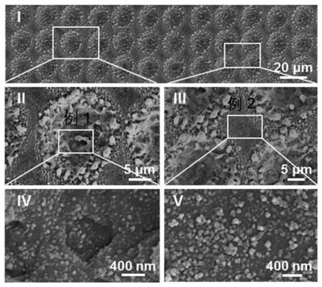
[0044] The substrate is n-type single crystal silicon with a resistivity of 1-5Ω·cm. The sample was irradiated with a femtosecond laser system that generated laser pulses with a center wavelength of 800 nm, a pulse width of 104 fs, and a repetition rate of 1 kHz. Use a power of 5 mW to focus the laser beam perpendicular to the surface of these samples. The laser pulse is Gaussian, with a spot diameter of 14 μm at the focal plane. The high-speed inching of the laser is precisely controlled by the scanning galvanometer suitable for the laser system to generate a 5×5mm dot matrix on the Si substrate. The number of pulses per point can be selected between 8 and 40.

[0045] Next, the substrate was ultrasonically cleaned with ethanol and ultrapure water for 10 minutes, respectively. Afterwards, the samples were dried in a vacuum oven at 100 °C for 20 min.

[0046] Subsequently, Ag films with thicknesses of 50.1 nm, 92.7 nm, 161.6 nm, 225.5 nm, and 282.9 nm were deposited on th...


PUM

PropertyMeasurementUnit
particle diameteraaaaaaaaaa
thicknessaaaaaaaaaa
diameteraaaaaaaaaa

Abstract

The invention provides a preparation method of a surface-enhanced Raman substrate with a layered micro / nano structure, which comprises the following steps: irradiating the surface of a silicon or silicon dioxide substrate by using nanosecond to femtosecond laser pulses to form a micro-pit array; cleaning and drying the substrate on which the micro-pit array is formed; and depositing and forming asilver film in the micro-pit array area of the substrate. According to the method, the MA-SERS with the layered micro / nano structure can be prepared through laser treatment from nanosecond to femtosecond and magnetron sputtering; the prepared MA-SERS has good wettability, the contact angle is about 150 degrees, Meanwhile, the enhancement factor of surface enhanced Raman scattering can reach 1.3 *10 < 7 > and is sufficient to detect the molecular level; the preparation process is economical and efficient; the prepared MA-SERS has a wide application prospect in detection of biological medicines, pesticide residues and an ultralow-concentration solution polluted by the environment.

Description

technical field [0001] The invention relates to the technical field of Raman detection of trace substances, in particular to a method for preparing a surface-enhanced Raman substrate with a layered micro / nano structure. Background technique [0002] Generally speaking, surface-enhanced Raman scattering with unique molecular vibrational fingerprints is used to identify analytes, providing an effective non-invasive spectroscopic method for the detection of trace molecules in the biomedical / analytical field. [0003] However, although considerable efforts have been invested in developing various SERS substrates with hierarchical micro / nanostructures to obtain sufficient sensitivity while maintaining appropriate superhydrophobicity, it is still difficult to integrate superhydrophobicity and Combining hotspots with plasmonic nanostructures remains a challenge. Contents of the invention [0004] The purpose of the present invention is to solve at least one of the above-mentione...

Claims


Application Information

Patent Timeline
Patent Type & Authority Applications(China)
IPC IPC(8): G01N21/65
CPCG01N21/658Y02P70/50
Inventor 李晓红程辉李国强肖林方佳浩唐晓轩马浩宇李青山谭诗莹
Owner SOUTHWEAT UNIV OF SCI & TECH
Why Eureka
Try Eureka