
Integrated optical beam splitter

A technology of integrated optics and beam splitters, applied in optics, optical components, light guides, etc., can solve problems such as chip performance degradation, irreversible damage to optical structures, and decline in chip integration

Inactive Publication Date: 2020-05-19
CHINA SCI PHOTON CHIP HAINING TECH CO LTD
View PDF3 Cites 7 Cited by
  • Summary
  • Abstract
  • Description
  • Claims
  • Application Information

AI Technical Summary

Problems solved by technology

When the power density in the optical waveguide is too high, the nonlinear effects of the optical waveguide, such as two-photon absorption and Kerr effect, will increase chip loss and signal distortion, resulting in chip performance degradation
When the power density exceeds the integrated waveguide damage threshold, it will cause irreversible damage to the optical structure
Reducing the power density in the waveguide requires increasing the effective mode field area of ​​the waveguide, which will increase the bending radius of the waveguide and reduce the integration of the chip
[0006] In the prior art, the silicon / silicon dioxide, or silicon nitride / silicon dioxide material system has a relatively high refractive index contrast, and the single-mode waveguide in the optical communication C-Band mode field area is usually below 0.5um^2, and the bending radius 5um-100um, high integration, but low nonlinear effect threshold; doped silica system with low refractive index contrast, single-mode waveguide C-Band mode field area can reach more than 80um^2, nonlinear effect threshold is relatively low High, but the integration level is low, the waveguide bending radius is on the order of millimeters, and the chip size is large
[0007] In summary, it is difficult to manufacture a silicon-based optical chip that can withstand high-power beams and has a high degree of integration based on existing technologies

Method used


Image

  • Integrated optical beam splitter
  • Integrated optical beam splitter
  • Integrated optical beam splitter

Examples


Embodiment Construction

[0027] Embodiments of the present invention are described in detail below, examples of which are shown in the drawings, wherein the same or similar reference numerals designate the same or similar elements or elements having the same or similar functions throughout. The embodiments described below by referring to the figures are exemplary only for explaining the present invention and should not be construed as limiting the present invention.

[0028] In describing the present invention, it should be understood that the terms "center", "longitudinal", "transverse", "upper", "lower", "front", "rear", "left", "right", " The orientations or positional relationships indicated by "vertical", "horizontal", "top", "bottom", "inner" and "outer" are based on the orientations or positional relationships shown in the drawings, and are only for the convenience of describing the present invention and Simplified descriptions, rather than indicating or implying that the device or element refe...


PUM


Abstract

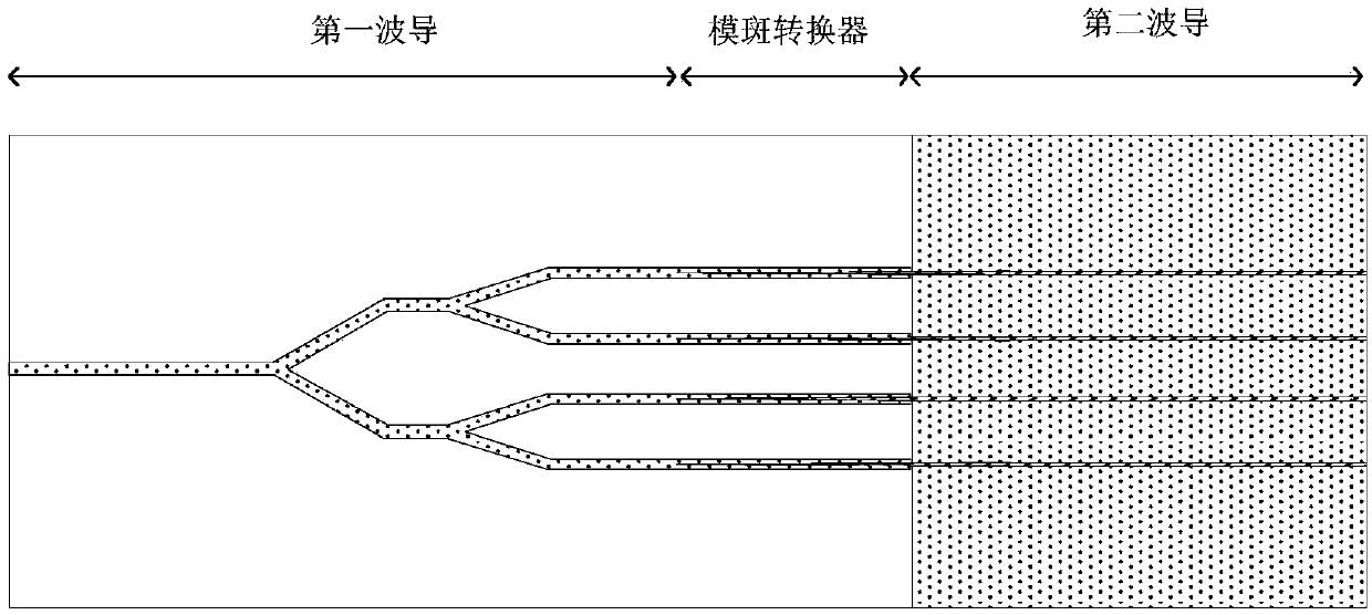
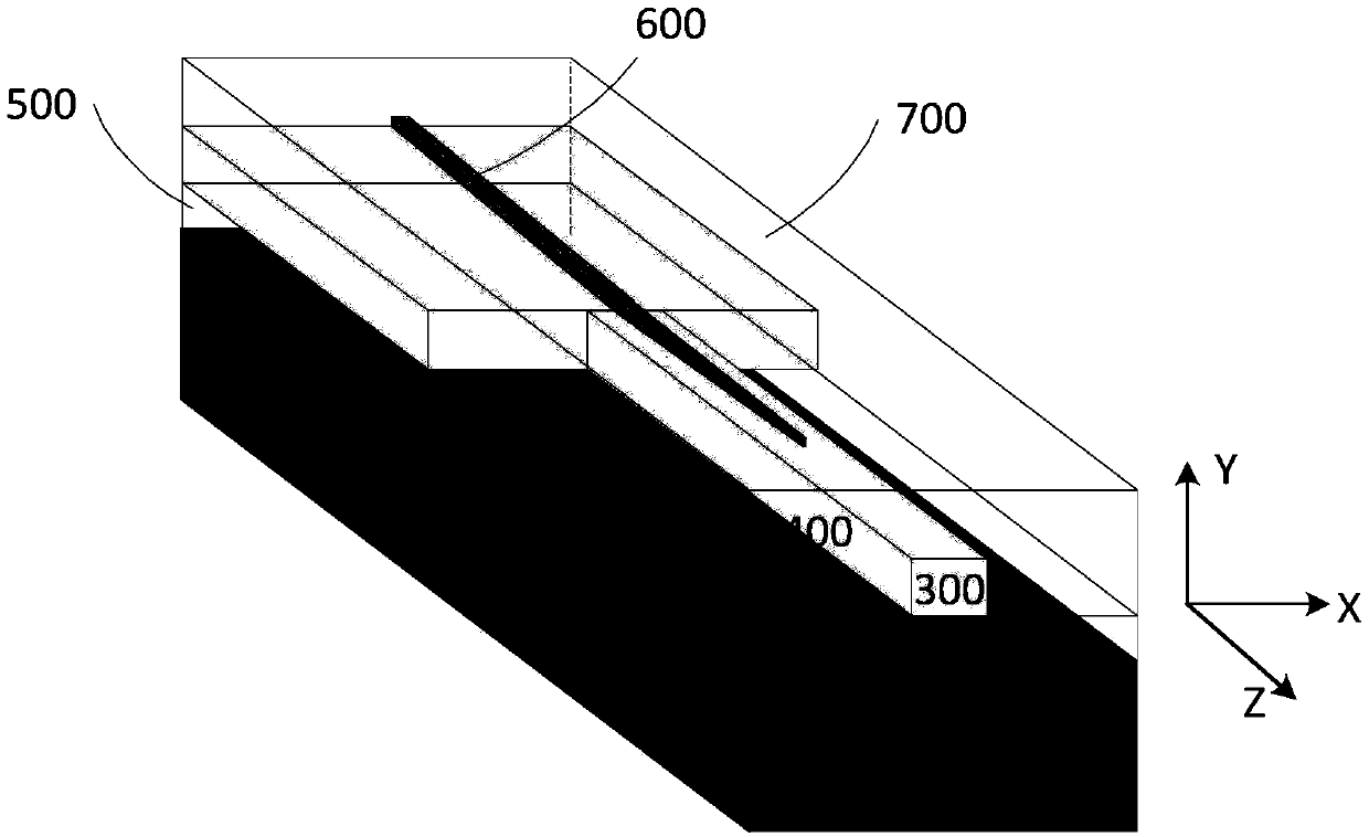
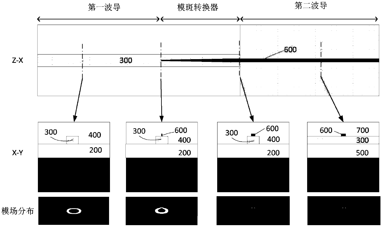
The invention discloses an integrated optical beam splitter. The integrated optical beam splitter comprises a first waveguide, a second waveguide and a mode spot converter, wherein a refractive indexcontrast of the second waveguide is higher than that of the first waveguide; the mode spot converter is arranged between the first waveguide and the second waveguide and is used for realizing mode conversion between the first waveguide and the second waveguide; the first waveguide includes an input waveguide and a beam splitting structure, and the first waveguide includes a first lower cladding, afirst core layer and a first upper cladding which are arranged in sequence; the second waveguide includes an output waveguide; the second waveguide includes a second lower cladding, a first core layer, a second core layer and a second upper cladding which are arranged in sequence; and the mode spot converter includes the first lower cladding, the first core layer, a second core layer, and the first upper cladding. The beam splitter has advantages that an input end of the beam splitter can be coupled with a standard single-mode optical fiber in a low-loss manner, and has a high optical nonlinear threshold value; and an output part of the beam splitter can be coupled with a high-integration-level functional device in the low-loss manner.

Description

technical field [0001] The invention relates to the technical field of optical chips, in particular to an integrated optical beam splitter. Background technique [0002] Silicon-based integrated optical chips use single crystal silicon as the substrate material, and form waveguide cladding and core layer structures through epitaxial growth, deposition, bonding, doping, etc. etc. to realize the transfer of waveguide patterns, and finally prepare integrated devices and systems with optoelectronic functions. [0003] Compared with traditional space or fiber optic devices, silicon-based integrated optical chips have the advantages of optoelectronic integration, compact structure, wide source of materials, compatibility with microelectronic processes, easy mass production, and low cost. With the maturity of microelectronic CMOS technology, the application of silicon-based integrated optical chips in optical communication, sensing, display, computing and other fields has graduall...

Claims


Application Information

Patent Timeline
Patent Type & Authority Applications(China)
IPC IPC(8): G02B6/12G02B6/122
CPCG02B6/12G02B6/1228G02B2006/1215
Inventor 刘敬伟李文玲田立飞张新群
Owner CHINA SCI PHOTON CHIP HAINING TECH CO LTD
Learn More