Method for embedding chips into cavities in front and back sides of adapter plate

An adapter plate and cavity technology, which is applied to the field of embedding chips on the front and back sides of the adapter plate, can solve the problems of complex process and high cost, and achieve the effects of large economic benefits, large cost advantages and broad application prospects.

Active Publication Date: 2020-06-16
ZHEJIANG UNIV
View PDF20 Cites 20 Cited by
  • Summary
  • Abstract
  • Description
  • Claims
  • Application Information

AI Technical Summary

Problems solved by technology

In addition, for the adapter board with double-layer chip structure, it is generally necessary to make a double-layer adapter board, then embed different chips into each layer of the adapter board, and then perform wafer-level bonding on the adapter board. The process is complicated and higher cost

Method used


Image

  • Method for embedding chips into cavities in front and back sides of adapter plate
  • Method for embedding chips into cavities in front and back sides of adapter plate
  • Method for embedding chips into cavities in front and back sides of adapter plate

Examples


Embodiment 1

[0057] include:

[0058] A: TSV (Through Silicon Via) is made on a silicon wafer with a double-layer SOI (Silicon-On-Insulator, silicon on insulating substrate) layer, and the TSV stops on the surface of the second layer of SOI, and the TSV is filled with electroplating metal;

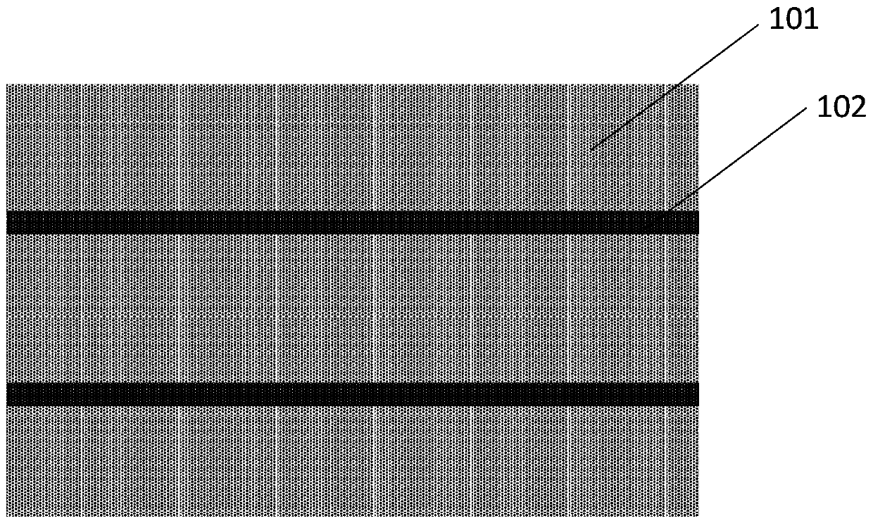
[0059] like figure 1 As shown, an SOI silicon wafer 101 is selected, wherein 102 is an SOI layer. This silicon wafer has two layers of SOI, from top to bottom, which are the first SOI layer 102 and the second SOI layer;

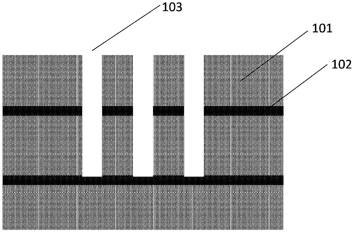
[0060] like figure 2 As shown, TSV holes 103 are fabricated on the surface of the SOI silicon wafer by photolithography and etching processes, the hole diameter ranges from 1um to 1000um, and the depth ranges from 10um to 1000um;

[0061] Etching stops on the second SOI layer;

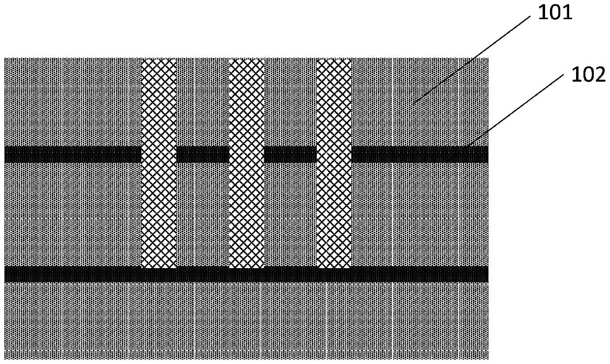
[0062] like image 3 As shown, an insulating layer such as silicon oxide or silicon nitride is deposited on the silicon wafer, or directly thermally oxidized, and the thickness of the insulating layer ran...

Embodiment 2

[0074] include:

[0075] A: Make TSV on the silicon wafer with double-layer SOI layer, TSV stops on the surface of the second layer of SOI, continue to etch the TSV to the lower surface of the SOI, and fill the TSV with metal plating;

[0076] like Figure 11 As shown, the SOI silicon wafer is selected. This silicon wafer has two layers of SOI; TSV holes are made on the surface of the SOI silicon wafer through photolithography and etching processes. The diameter of the hole ranges from 1um to 1000um, and the depth ranges from 10um to 1000um;

[0077] Etching the TSV stops at the surface of the second layer of SOI, and continues to etch the TSV to the lower surface of the SOI;

[0078] Deposit insulating layers such as silicon oxide or silicon nitride on the silicon wafer, or direct thermal oxidation, the thickness of the insulating layer ranges from 10nm to 100um; make seeds on the insulating layer by physical sputtering, magnetron sputtering or evaporation process Layer, th...


PUM

PropertyMeasurementUnit
thicknessaaaaaaaaaa
thicknessaaaaaaaaaa
thicknessaaaaaaaaaa

Abstract

The invention discloses a method for embedding chips into cavities in the front and back sides of an adapter plate. The method comprises the steps that the adapter plate adopts a silicon wafer with double SOI (silicon on insulator) layers to manufacture a silicon through hole, the silicon through hole penetrates through a first SOI layer and stops on a second SOI layer to obtain the silicon waferwith the silicon through hole, and then the silicon through hole is filled with electroplated metal to obtain the silicon wafer filled with metal; a groove is etched on the opening surface of the silicon through hole, a metal column in the groove is corroded, and cavities are formed on the front side and the back side to obtain the adapter plate with grooves on the two sides; and the chips with soldering tin are embedded, then an RDL interconnection layer is manufactured on the surface, a second SOI layer is continuously etched to expose one end of the metal column filled in the silicon through hole, the chips with soldering tin balls are embedded, the filling colloid is solidified, and the surface colloid is removed. According to the invention, the adapter plate is manufactured, and the grooves are formed in the front side and the back side of the adapter plate; chips are embedded into the grooves; and the purpose that the chips are embedded into the front side and the back side of the adapter plate is achieved.

Description

technical field [0001] The invention relates to the technical field of chip packaging, in particular to a method for embedding chips in cavities on the front and back sides of an adapter board. Background technique [0002] Millimeter wave radio frequency technology is developing rapidly in the semiconductor industry. It is widely used in high-speed data communication, automotive radar, airborne missile tracking system, and space spectrum detection and imaging. It is expected that the market will reach 1.1 billion US dollars in 2018 and become an emerging industry. New applications put forward new requirements for the electrical performance, compact structure and system reliability of products. For wireless transmitting and receiving systems, they cannot be integrated into the same chip (SOC). Therefore, it is necessary to integrate different chips including radio frequency Units, filters, power amplifiers, etc. are integrated into an independent system to realize the functi...

Claims


Application Information

Patent Timeline
Patent Type & Authority Applications(China)
IPC IPC(8): H01L21/768H01L21/50H01L21/56H01L21/60
CPCH01L21/76898H01L21/50H01L21/56H01L24/80
Inventor 郁发新冯光建王志宇张兵
Owner ZHEJIANG UNIV
Why Eureka
Try Eureka