Erbium silicate crystal and silicon nanocrystalline co-inlaid silicon dioxide film and preparation method and application thereof

A silicon nanocrystal and silicon dioxide technology, which is applied in the field of co-embedded silicon dioxide film of erbium silicate crystal and silicon nanocrystal and its preparation, can solve the problem that erbium silicate crystal and silicon nanocrystal cannot be obtained at the same time, and achieves the Avoid the effects of uneven film distribution, avoid concentration quenching, and low turn-on voltage

Active Publication Date: 2020-06-19
ZHEJIANG UNIV
View PDF1 Cites 5 Cited by
  • Summary
  • Abstract
  • Description
  • Claims
  • Application Information

AI Technical Summary

Problems solved by technology

The above results show that it is impossible to obtain erb...

Method used


Image

  • Erbium silicate crystal and silicon nanocrystalline co-inlaid silicon dioxide film and preparation method and application thereof
  • Erbium silicate crystal and silicon nanocrystalline co-inlaid silicon dioxide film and preparation method and application thereof
  • Erbium silicate crystal and silicon nanocrystalline co-inlaid silicon dioxide film and preparation method and application thereof

Examples


Embodiment Construction

[0038]The present invention will be further described below in conjunction with the accompanying drawings and specific embodiments. It should be understood that these examples are only used to illustrate the present invention and are not intended to limit the scope of the present invention. The operating methods not indicated in the following examples are generally in accordance with conventional conditions, or in accordance with the conditions suggested by the manufacturer.

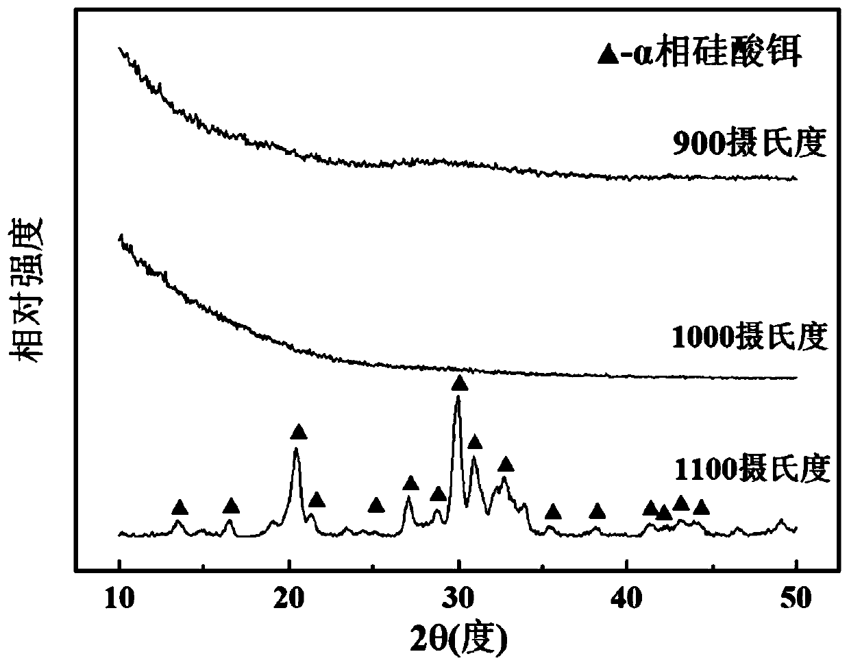
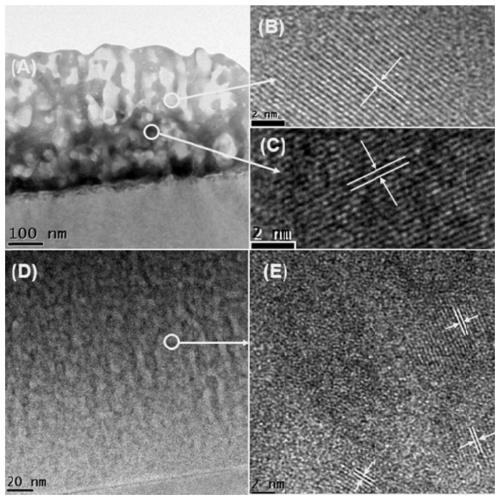
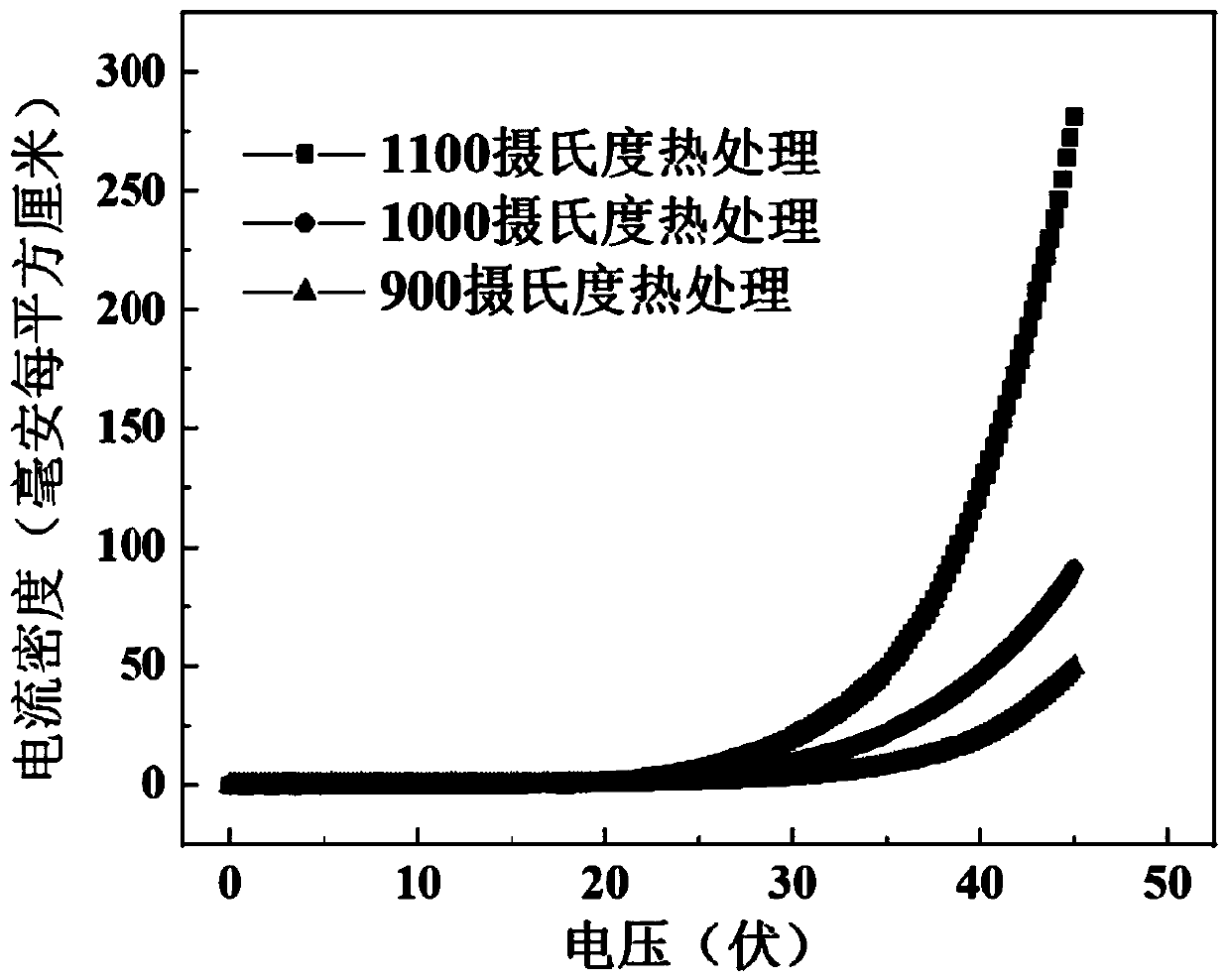
[0039] In this embodiment, the electroluminescent device based on the thin film preparation of erbium silicate grains and silicon nanocrystals co-embedded silicon dioxide adopts radio frequency magnetron sputtering to (100) single-sided polishing resistivity ρ= 0.1~1Ω.cm P-type Czochralski single crystal silicon wafer sputtering film, the substrate heating temperature is 300°C when sputtering the film, and the vacuum degree of the background of the radio frequency sputtering equipment is 2×10 - 3 Pa, t...


PUM


Abstract

The invention discloses an erbium silicate crystal and silicon nanocrystal co-inlaid silicon dioxide film and a preparation method and application thereof. A silicon-rich erbium silicate film is prepared by reactive co-sputtering, and the erbium silicate crystal and the silicon nanocrystal are obtained by high-temperature heat treatment. The invention also discloses a low-turn-on-voltage high-efficiency infrared light emitting diode prepared on the basis of the film. Due to the formation of the silicon nanocrystals, the conductivity of the film is enhanced, and the device turn-on voltage is reduced. Due to the formation of the erbium silicate crystal, the effective doping concentration of film erbium is improved, the infrared electroluminescence intensity of the device is improved, and theefficiency is greatly improved. The method is simple in preparation process and good in industrial compatibility, and has a wide application prospect in the fields of silicon-based integrated light source or semiconductor light emitting, optical communication and the like.

Description

technical field [0001] The invention relates to the technical field of silicon-based optoelectronics, in particular to a silicon dioxide film co-embedded with erbium silicate crystals and silicon nanocrystals and its preparation method and application. Background technique [0002] With the rapid development of the microelectronics industry with Moore's Law, there are more and more transistors on a single chip, and the problems of signal delay, heat release and signal interference caused by traditional metal wire interconnection are becoming more and more obvious. Optical interconnection Due to its advantages of fast signal transmission speed, low loss and no interference, it has become an inevitable trend in the development of integrated circuits. [0003] At present, silicon-based optical interconnects have made great progress in optical waveguides, optical signal modulators, optical signal amplifiers, and optical signal detectors. Only efficient light sources, especially ...

Claims


Application Information

Patent Timeline
IPC IPC(8): C30B25/06C30B28/14C30B29/06C30B29/34C23C14/35C23C14/10C23C14/58C23C14/16C23C14/08H01L33/00B82Y30/00
CPCB82Y30/00C23C14/0036C23C14/086C23C14/10C23C14/165C23C14/5806C30B25/06C30B28/14C30B29/06C30B29/34H01L33/005H01L33/0054
Inventor 李东升何马军杨德仁
Owner ZHEJIANG UNIV
Why Eureka
Try Eureka