SA-LIGBT device with longitudinally separated anode

An anode and device technology, applied in the field of power semiconductor devices, can solve the problems of transistor voltage rebound, uneven current distribution of transistors, affecting device reliability, etc., so as to reduce turn-off loss, increase anode short-circuit resistance, and improve on-voltage drop effect

Active Publication Date: 2020-06-23
CHONGQING UNIV OF POSTS & TELECOMM
View PDF10 Cites 2 Cited by
  • Summary
  • Abstract
  • Description
  • Claims
  • Application Information

AI Technical Summary

Problems solved by technology

However, the introduction of the N+ anode will also cause the transistor to switch from unipolar conduction mode to bipolar mode when it is turned on, causing the transistor to produce a voltage rebound phenomenon, that is, the snapback effect
The Snapback effect will make the current distribution of the transistor uneven and seriously affect the reliability of the device.

Method used


Image

  • SA-LIGBT device with longitudinally separated anode
  • SA-LIGBT device with longitudinally separated anode
  • SA-LIGBT device with longitudinally separated anode

Examples


Embodiment example 1

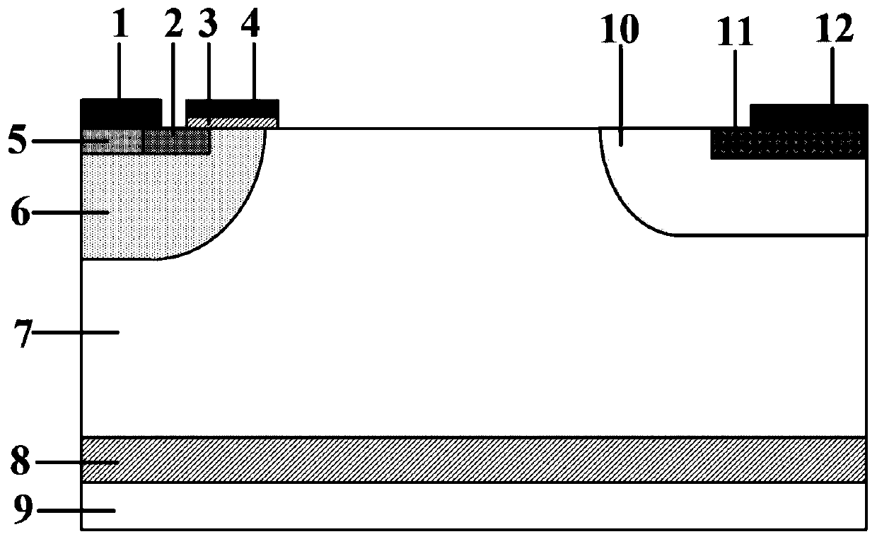
[0039] Such as Figure 5 As shown, a SA-LIGBT device with a vertically separated anode structure, its features include: cathode metal 1, N-type heavily doped cathode region 2, gate oxide layer 3, gate 4, P-type heavily doped cathode region 5 , P-body6, N-type drift region 7, insulating dielectric layer 8, P-type substrate 9, N-type buffer layer 10, P-type heavily doped anode region 11, anode metal 12, anode dielectric isolation layer 13, N-type heavy Doping the anode region 14 and the P-type floating layer 15 .

[0040] The P-type substrate 9, insulating dielectric layer 8 and N-type drift region 7 form an SOI structure. The P-type substrate is P-type doped silicon, and its thickness and doping concentration have a very wide selection range; the material of the insulating dielectric layer 8 is silicon dioxide with a thickness of 0.5 μm to 5 μm.

[0041] The N-type drift region 7 is covered on the insulating dielectric layer 8, and the N-type drift region 7 is silicon with a ...

Embodiment example 2

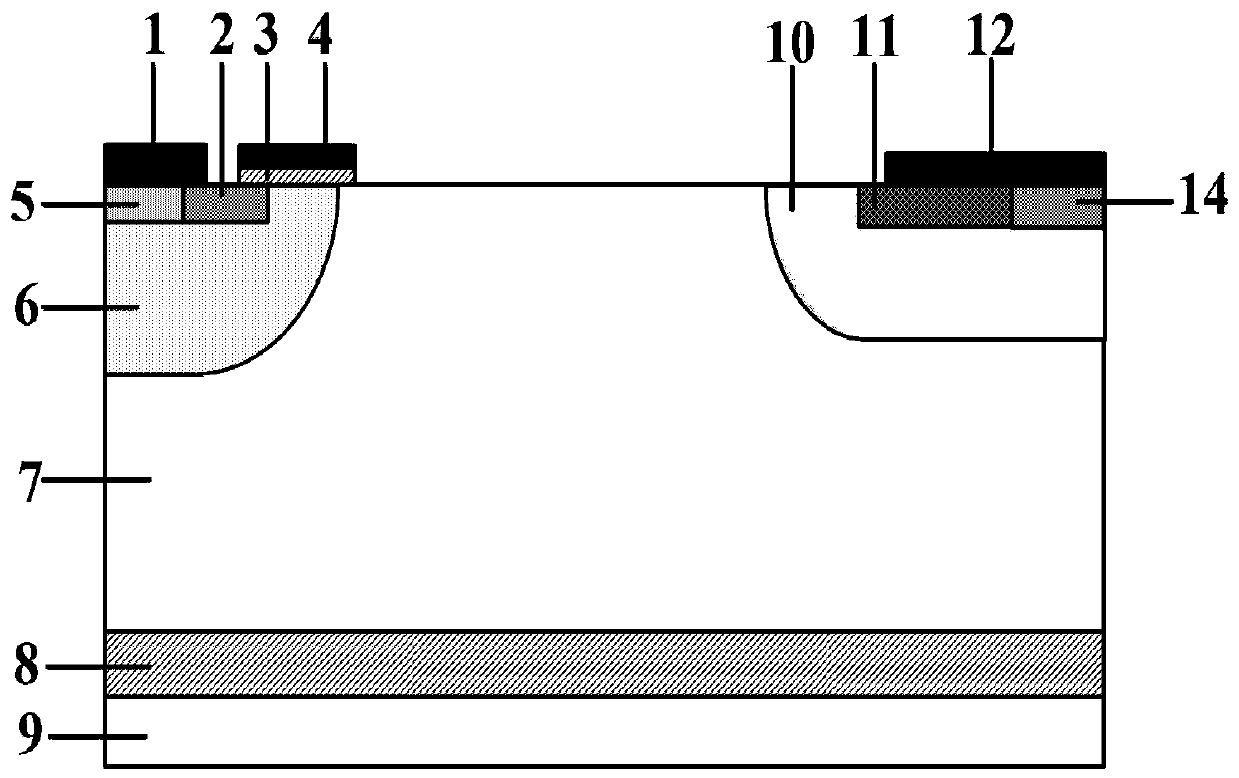
[0050] Such as Image 6 As shown, this example provides a SA-LIGBT device with a vertically separated anode structure. This implementation case is based on the implementation case 1, and the P-type floating layer 15 under the N-type heavily doped anode region 14 is removed. . The specific implementation plan is as follows:

[0051] A SA-LIGBT device with a vertically separated anode structure, which is characterized by: cathode metal 1, N-type heavily doped cathode region 2, gate oxide layer 3, gate 4, P-type heavily doped cathode region 5, P- body6, N-type drift region 7, insulating dielectric layer 8, P-type substrate 9, N-type buffer layer 10, P-type heavily doped anode region 11, anode metal 12, anode dielectric isolation layer 13, N-type heavily doped anode District 14.

[0052] The P-type substrate 9, insulating dielectric layer 8 and N-type drift region 7 form an SOI structure. The P-type substrate is P-type doped silicon, and its thickness and doping concentration ...

Embodiment example 3

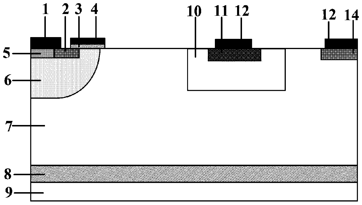
[0061] Such as Figure 7 As shown, this example provides a SA-LIGBT device with a vertically separated anode structure. On the basis of Embodiment 2, a P-type floating layer 15 is introduced directly below the anode dielectric isolation layer. The specific implementation plan is as follows:

[0062] Its features include: cathode metal 1, N-type heavily doped cathode region 2, gate oxide layer 3, gate 4, P-type heavily doped cathode region 5, P-body6, N-type drift region 7, insulating dielectric layer 8, P-type substrate 9 , N-type buffer layer 10 , P-type heavily doped anode region 11 , anode metal 12 , anode dielectric isolation layer 13 , N-type heavily doped anode region 14 , and P-type floating layer 15 .

[0063] The P-type substrate 9, insulating dielectric layer 8 and N-type drift region 7 form an SOI structure. The P-type substrate is P-type doped silicon, and its thickness and doping concentration have a very wide selection range; the material of the insulating diel...


PUM

PropertyMeasurementUnit
Thicknessaaaaaaaaaa
Thicknessaaaaaaaaaa
Thicknessaaaaaaaaaa

Abstract

The invention relates to an SALIGBT device with a longitudinally separated anode structure, and belongs to the field of semiconductor power devices. According to the invention, the N+ anode and the P+anode of a traditional SA-LIGBT are separated, the N+ anode is arranged in the device, and the flow path of electrons in a unipolar conductive mode is prolonged by increasing the longitudinal depth of the N+ anode; a P-type floating layer below the N+ anode can increase the anode distribution resistance of the device, and the snapback effect is completely eliminated by adjusting the longitudinaldepth of the N+ anode and the doping concentration of the P-type floating layer. According to the invention, the longitudinal length of the device is utilized to reduce the chip area; the forward conduction voltage drop of the LIGBT with the new structure is 0.91V during forward conduction, which is reduced by 6.2% and 24% respectively compared with a separated anode short circuit type LIGBT and aconventional anode short circuit type LIGBT; and when the LIGBT is turned off, the N+ anode can rapidly extract electrons in a drift region, and the turn-off time of the N+ anode is 370ns and is reduced by 82% and 23% compared with a traditional LIGBT and a dielectric isolation type LIGBT.

Description

technical field [0001] The invention belongs to the field of power semiconductor devices and relates to a SA-LIGBT device with vertically separated anodes. Background technique [0002] Lateral Insulated Gate Bipolar Transistor (LIGBT) is a common bipolar power semiconductor device, which has the advantages of high input impedance, low conduction voltage and simple driving circuit. It is widely used in communication technology, new energy equipment and various consumer electronics fields. The traditional LIGBT device is improved from LDMOS (Lateral Double-diffused Metal-Oxide Semiconductor). The inventor replaced the N+ of the LDMOS drain with P+, turning the unipolar device into a bipolar device. Due to the introduction of P+, LIGBT can inject holes into the drift region when it is turned on, so that the conductance modulation effect occurs in the high-resistance drift region, thereby obtaining a higher current density. However, the large number of carriers stored in the ...

Claims


Application Information

Patent Timeline
IPC IPC(8): H01L29/739H01L29/06H01L29/08
CPCH01L29/7394H01L29/0808H01L29/0688
Inventor 陈伟中李顺黄垚黄元熙黄义贺利军张红升
Owner CHONGQING UNIV OF POSTS & TELECOMM
Why Eureka
Try Eureka