Material physical vapor deposition method and facility

A physical vapor deposition and equipment technology, which is applied in metal material coating process, ion implantation plating, coating, etc., can solve problems such as strong ion bombardment, high film stress non-uniformity, and poor stress at the edge and center of the wafer.

Active Publication Date: 2020-06-30
BETONE TECH SHANGHAI
View PDF12 Cites 7 Cited by
  • Summary
  • Abstract
  • Description
  • Claims
  • Application Information

AI Technical Summary

Problems solved by technology

[0003] The intra-chip stress non-uniformity of thin films is often high for conventional PVD systems because the specially designed permanent magnet setup for good film thickness uniformity tends to cause a greater degree of inhomogeneity at the edge of the target. ionization, resulting in stronger ion bombardment at the edge of the wafer, resulting in a very noticeable stress difference between the edge and center of the wafer;

Method used


Image

  • Material physical vapor deposition method and facility
  • Material physical vapor deposition method and facility
  • Material physical vapor deposition method and facility

Examples


Embodiment Construction

[0059] The present invention will be further described below in conjunction with accompanying drawing and embodiment;

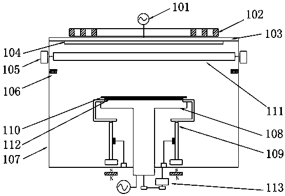
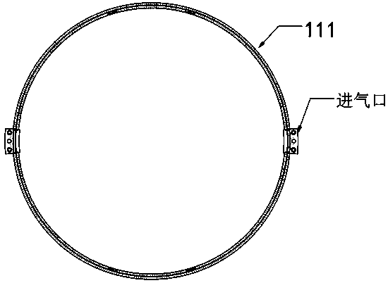
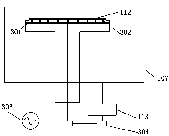
[0060] figure 1 As shown, the present invention provides a physical vapor deposition equipment for depositing metal oxides or metal nitrides on the surface of the wafer 110 carried by the tray 112 through DC, AC or pulsed DC magnetron sputtering, including a magnetron sputtering device , electromagnetic coil 105 , soft magnetic ring 106 , cavity 107 , intake ring 111 , tray 112 , wafer 110 , heating plate device 108 , motor 113 and wafer rotating device 109 . The magnetron sputtering device is installed above the cavity 107, the electromagnetic coil 105 is installed on the periphery of the cavity 107, the soft magnetic ring 106 is installed inside the cavity, at the same height or below the target 103, and the wafer 110 is placed on the tray 112 Above, the tray 112 is placed on the heating plate assembly 108 , and the heating plate assembly 108 and the wafer...


PUM


Abstract

The invention provides a material physical vapor deposition method and facility, and provides the method which is characterized in that a metal nitride or metal oxide film is deposited on the surfaceof a wafer by a permanent magnet device in a cavity through direct-current or alternating-current or pulse direct-current magnetron sputtering operation. The permanent magnet device cooperates with anelectromagnetic coil and a soft magnet ring to generate a primary magnetic field and a secondary magnetic field. The reaction gas used by film deposition operation enters the interior of the cavity through a gas inlet ring. The wafer is placed on a heating disc device, and the rotation of the wafer is achieved by a wafer rotating device. The heating disc device can control the temperature in a zonal mode. A permanent magnet or electromagnet device installed on a heating disc can form an extra secondary magnetic field, and the uniformity of the film thickness and the stress can be improved through the extra secondary magnetic field.

Description

technical field [0001] The invention relates to the field of manufacturing integrated circuits and micromechanical sensors, in particular to methods and equipment for physical vapor deposition materials. Background technique [0002] At present, many devices related to integrated circuits and micro-electromechanical systems (such as infrared night vision devices, storage capacitor devices, piezoelectric MEMS sensor devices, bulk acoustic wave devices and radio frequency resistor devices, etc.) need to use metal nitride and oxide things. In the above-mentioned devices, in order to ensure the reliability, stability and product consistency of the device performance, the non-uniformity of the deposited nitride and oxide film thickness is generally required to be controlled at about 1% or even lower, and the on-chip Stress uniformity requirements should be as low as possible. For example, bulk acoustic wave devices and piezoelectric MEMS sensor devices have extremely high requir...

Claims


Application Information

Patent Timeline
IPC IPC(8): C23C14/35C23C14/50C23C14/54C23C14/08C23C14/06
CPCC23C14/35C23C14/505C23C14/541C23C14/08C23C14/0641
Inventor 周云睢智峰张德培
Owner BETONE TECH SHANGHAI
Why Eureka
Try Eureka