Terahertz wave light-operated modulator and preparation method thereof

A modulator and terahertz technology, applied in the terahertz field, can solve the problems of high device manufacturing cost, complex processing, low operating frequency, etc., and achieve the effect of switching effect

Pending Publication Date: 2020-07-10
SHENZHEN INST OF ADVANCED TECH
View PDF8 Cites 1 Cited by
  • Summary
  • Abstract
  • Description
  • Claims
  • Application Information

AI Technical Summary

Problems solved by technology

However, the current modulation and detection technology of terahertz waves is still immature. For example, there are problems such as low modulation rate, low operating frequency, high device manufacturing cost, high material cost, and complicated processing.

Method used


Image

  • Terahertz wave light-operated modulator and preparation method thereof
  • Terahertz wave light-operated modulator and preparation method thereof
  • Terahertz wave light-operated modulator and preparation method thereof

Examples


Embodiment 1

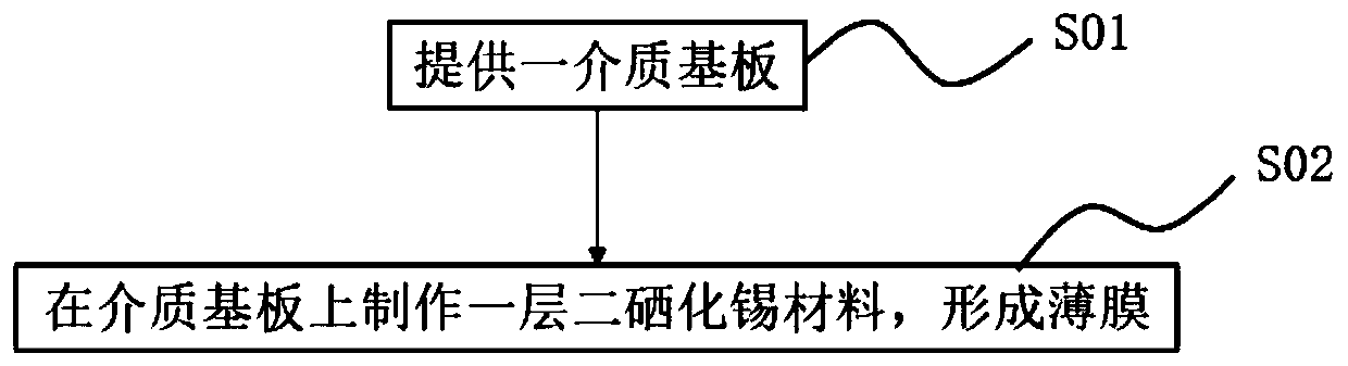
[0048] refer to figure 1 , the invention provides a preparation method of a terahertz wave optical control modulator, which mainly includes:

[0049] S01 , providing a dielectric substrate 10 .

[0050] The preparation process of the dielectric substrate 10 specifically includes:

[0051] Take a piece of high-resistance silicon wafer (such as 4 inches in size), clean it with hydrofluoric acid with a concentration between 4% and 8%, and soak it in hydrofluoric acid for 5min-10min to remove the oxide on the surface of the high-resistance silicon wafer ;

[0052] Then rinse the high-resistance silicon wafer with deionized water, dry it with nitrogen, and place it in a vacuum environment to prevent it from being oxidized by air again.

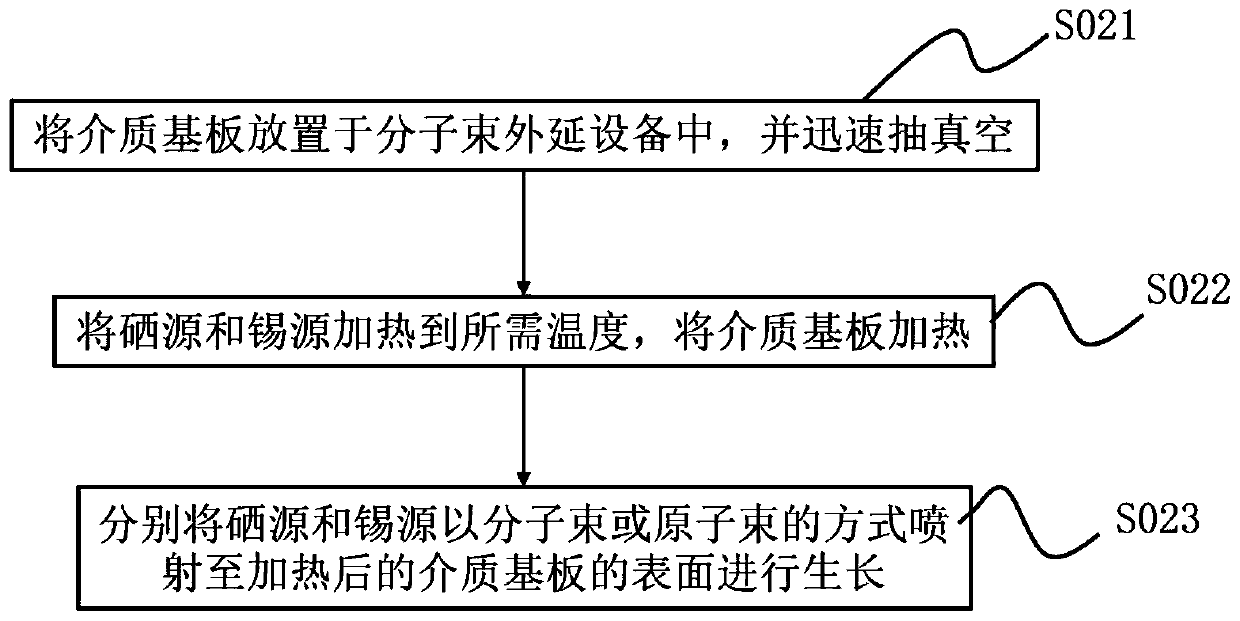
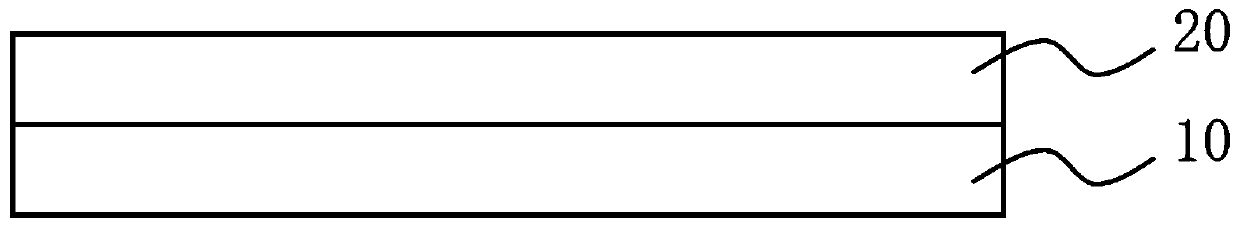
[0053] S02 , fabricating a layer of tin diselenide material on the dielectric substrate 10 to form a thin film 20 attached to the surface of the dielectric substrate 10 .

[0054] In this embodiment, the thin film 20 is grown by molecular beam ...

Embodiment 2

[0068] The tin diselenide material of the thin film 20 can be in several sheet structures standing on the surface of the dielectric substrate 10 .

[0069] Such as Figure 5 As shown, different from Embodiment 1, the steps of making a layer of tin diselenide material on the dielectric substrate 10 to form the thin film 20 in this embodiment include:

[0070] S021', prepare the nanoparticle of sheet-shaped tin diselenide.

[0071] This step can use the hot injection method, using the elemental selenium powder Se as the selenium source to obtain SnSe nanoparticles. When the amount of the Sn:Se precursor added is 1:2, the SnSe with a flaky shape can be generated. 2 of nanoparticles.

[0072] Preferably, the step S021' of preparing flake-shaped nanoparticles of tin diselenide specifically includes:

[0073] S0211', mix 1.152mmol selenium powder with 3ml oleylamine (OLA) and 1ml n-dodecanethiol, stir and heat to 60°C on a magnetic stirrer, so that Se is fully dissolved in OLA to...


PUM

PropertyMeasurementUnit
Impedance valueaaaaaaaaaa
Thicknessaaaaaaaaaa
Thicknessaaaaaaaaaa

Abstract

The invention discloses a preparation method of a terahertz wave light-operated modulator. The preparation method comprises the following steps: providing a dielectric substrate; and manufacturing a layer of tin diselenide material on the dielectric substrate to form a thin film attached to the surface of the dielectric substrate. The invention further provides a terahertz wave light-operated modulator which comprises a dielectric substrate and a film attached to the surface of the dielectric substrate. The dielectric substrate is used for transmitting terahertz waves, and the film is made oftin diselenide materials and used for being excited by terahertz light to generate photon-generated carriers. The terahertz wave modulator is prepared on the basis of the tin diselenide thin film, tindiselenide can be excited to generate photon-generated carriers when a pump light source irradiates the terahertz wave modulator, the number of excited carriers can be controlled by changing the light intensity, and therefore the switching effect of light-operated terahertz waves is achieved.

Description

technical field [0001] The invention relates to the field of terahertz technology, in particular to a terahertz wave optical control modulator and a preparation method thereof. Background technique [0002] Terahertz refers to radiation with a frequency of 0.1THz to 10THz on the electromagnetic spectrum, and its wavelength range is 0.03mm to 3mm, which is between microwaves and light waves, and is an intersecting field of electronics and photonics. Due to its independent properties such as transient, low energy and coherence, terahertz waves have great scientific value and broad application prospects in many fields such as nondestructive testing, wireless communication, and military radar. Moreover, due to the characteristics of the frequency band to which terahertz waves belong, terahertz wireless communication has the characteristics of rich frequency bands, good confidentiality, and strong anti-interference. However, the current modulation and detection technology of ter...

Claims


Application Information

Patent Timeline
IPC IPC(8): G02F1/01
CPCG02F1/0126G02F2203/13Y02P70/50
Inventor 姚琳李伟民杨春雷杨兵许述达谢芳梅王忠国
Owner SHENZHEN INST OF ADVANCED TECH
Why Eureka
Try Eureka