Manufacturing method of super-thick adapter plate
A production method and technology of adapter boards, which are applied in semiconductor/solid-state device manufacturing, electrical components, circuits, etc., can solve the problems of complex adapter boards, high input costs and production costs, and the lack of popularization of adapter boards. The effect of less production cost and convenient production
- Summary
- Abstract
- Description
- Claims
- Application Information
AI Technical Summary
Problems solved by technology
Method used
Image

Examples
specific Embodiment approach 1
[0049] An embodiment of the present invention provides a method for manufacturing an ultra-thick adapter plate, including the following steps:
[0050] A. Fabricate TSV on the surface of the double-layer SOI silicon wafer transfer board, fill the TSV with metal, thin the back of the transfer board, and make a groove on the back of the transfer board;
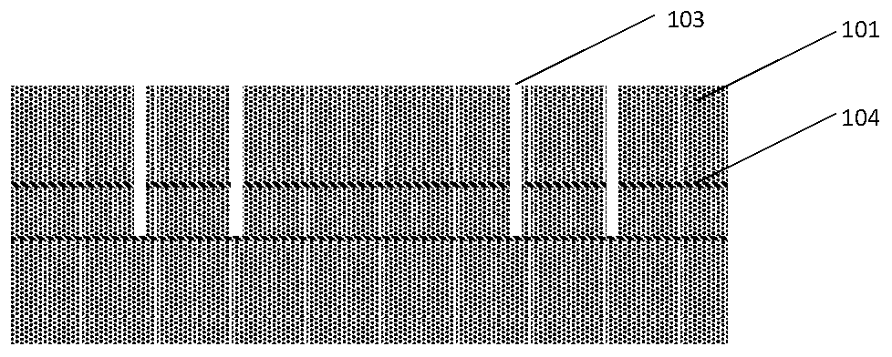
[0051] Such as Figure 1a As shown, a double-layer SOI silicon wafer 101 is prepared, and TSV103 is fabricated on the surface of the silicon wafer through photolithography and etching processes; the TSV stops on the second layer of SOI104, where the diameter of the TSV is between 1um and 1000um;
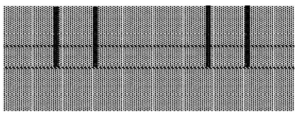
[0052] Such as Figure 1b As shown, a passivation layer such as silicon oxide or silicon nitride is deposited on the silicon wafer, or directly thermally oxidized, and the thickness of the passivation layer ranges from 10nm to 100um;
[0053] The seed layer is made on the insulating layer by physical sputtering, magnetron sputtering or evaporati...
specific Embodiment approach 2
[0068] An embodiment of the present invention provides a method for manufacturing an ultra-thick adapter plate, including the following steps:
[0069] A: Fabricate TSV on the surface of single-layer SOI silicon wafer transfer board, fill TSV with metal, thin the back of the transfer board, and make grooves on the back of the transfer board;
[0070] Such as Figure 1g As shown, TSV is fabricated on the surface of a single-layer SOI silicon wafer transfer board;
[0071] Such as Figure 1h As shown, the TSV is filled with metal;
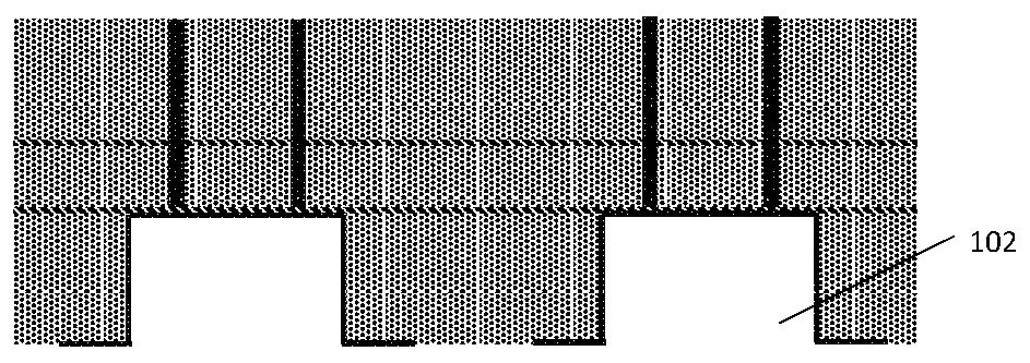
[0072] Such as Figure 1i As shown, thin the back of the adapter plate, and make a groove on the back of the adapter plate;
[0073] B: Electroplating metal in the groove, filling the cavity with colloid, and making RDL and pad on the groove surface;
[0074] Such as Figure 1i As shown, the metal is plated in the groove and the cavity is filled with colloid ( Figure 1k Shown), make RDL and pads on this side;
[0075] C: Cut the adapter board into a single chi...
PUM
| Property | Measurement | Unit |
|---|---|---|
| Thickness | aaaaa | aaaaa |
| Thickness | aaaaa | aaaaa |
| Diameter | aaaaa | aaaaa |
Abstract
Description
Claims
Application Information
 - R&D
- Intellectual Property
- Life Sciences
- Materials
- Tech Scout
- Unparalleled Data Quality
- Higher Quality Content
- 60% Fewer Hallucinations
Browse by: Latest US Patents, China's latest patents, Technical Efficacy Thesaurus, Application Domain, Technology Topic, Popular Technical Reports.
© 2025 PatSnap. All rights reserved.Legal|Privacy policy|Modern Slavery Act Transparency Statement|Sitemap|About US| Contact US: help@patsnap.com