An avalanche photodiode

A technology of avalanche photodiodes and diodes, applied in circuits, electrical components, semiconductor devices, etc., can solve problems such as the inability to take into account the linearity and responsivity performance of avalanche photodiodes, achieve both linearity and responsivity performance, and increase transit time , The effect of reducing the amount of electric field drop

Active Publication Date: 2022-02-15
HUAZHONG UNIV OF SCI & TECH
View PDF5 Cites 0 Cited by
  • Summary
  • Abstract
  • Description
  • Claims
  • Application Information

AI Technical Summary

Problems solved by technology

[0004] In view of the above defects or improvement needs of the prior art, the present invention provides an avalanche photodiode, which aims to solve the inability of the prior art to reduce the influence of the space charge effect by reducing the thickness of the depletion absorbing layer. Considering the problem of linearity and responsivity performance of avalanche photodiode

Method used


Image

  • An avalanche photodiode
  • An avalanche photodiode
  • An avalanche photodiode

Examples


Embodiment 1

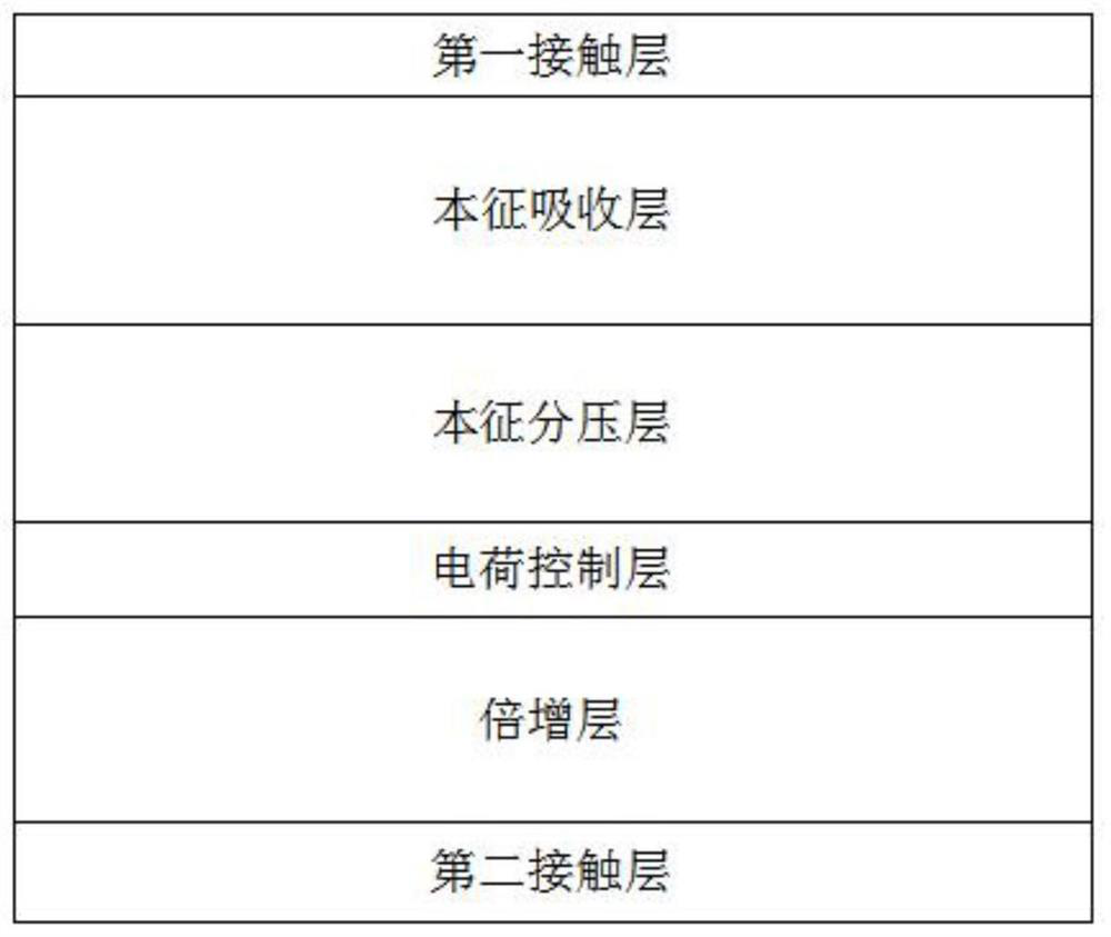
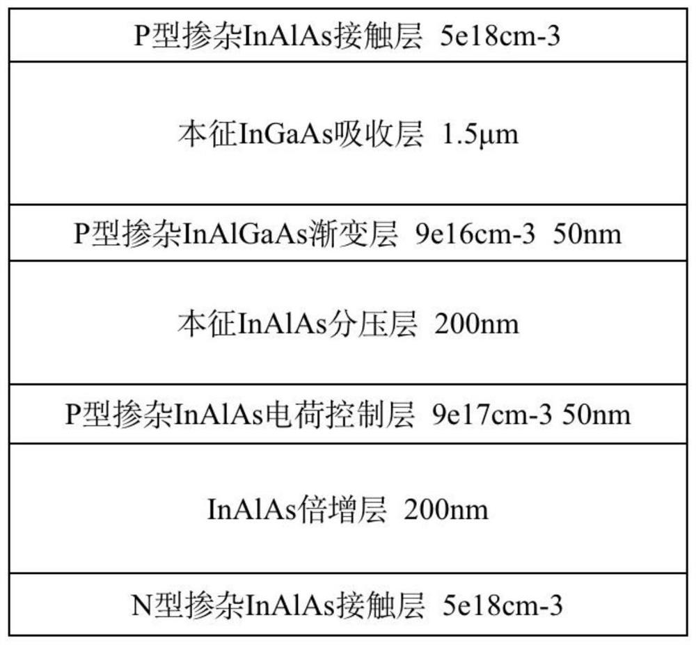
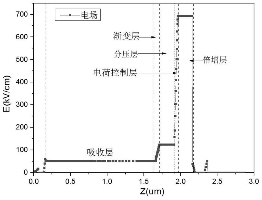
[0041] Take the III-V avalanche photodiode as an example for illustration, such as figure 2 As shown, it includes: P-type doped InAlAs contact layer, intrinsic InGaAs absorption layer, P-type doped InAlGaAs gradient layer, intrinsic InAlAs pressure dividing layer, P-type doped InAlAs charge control layer, InAlAs multiplication layer and N-type doped InAlAs contact layer;

[0042] Wherein, the P-type doped InAlAs contact layer is used to connect with the P-type electrode. The intrinsic InGaAs absorbing layer is used to absorb incident light to form electron-hole pairs; in this embodiment, the incident light is in the near-infrared band. The P-type doped InAlGaAs graded layer is used to slow down the energy band discontinuity between the intrinsic InGaAs absorption layer and the intrinsic InAlAs pressure dividing layer. The intrinsic InAlAs voltage divider is used to increase the thickness of the avalanche photodiode based on the relationship between the potential and the ele...

Embodiment 2

[0050] Taking silicon germanium avalanche photodiode as an example, as Figure 5As shown, including: P-type doped Si contact layer, intrinsically doped Ge absorbing layer, intrinsically doped Si voltage divider layer, P-type doped Si charge control layer, intrinsically doped Si multiplier layer and N-type doped Si contact layer. Compared with the III-V avalanche photodiode diode, the SiGe avalanche photodiode has no graded layer, and the intrinsically doped Si voltage divider layer is placed between the intrinsically doped Ge absorption layer and the P-type doped Si charge control layer. The function of each layer of the silicon germanium avalanche photodiode is similar to that of the III-V avalanche photodiode, and will not be repeated here.


PUM

PropertyMeasurementUnit
thicknessaaaaaaaaaa
thicknessaaaaaaaaaa

Abstract

The invention discloses an avalanche photodiode, which comprises: a first contact layer, an intrinsic absorption layer, an intrinsic voltage division layer, a charge control layer, a multiplication layer and a second contact layer distributed sequentially from top to bottom; An intrinsic voltage divider layer is added between the intrinsic absorption layer and the charge control layer. By using the intrinsic voltage divider layer, based on the relationship between the potential and the electric field, the relative distribution of the electric field of the absorption layer and the electric field of the multiplication layer is not affected. , increasing the thickness of the avalanche photodiode, thereby reducing the electric field drop of the multiplication layer due to the space charge effect of electron-hole pairs, and improving the linearity of the avalanche photodiode. At the same time, the present invention does not reduce the depletion The thickness of the absorbing layer and the high responsivity of the avalanche photodiode can take into account both the linearity and responsivity performance of the avalanche photodiode.

Description

technical field [0001] The invention belongs to the technical field of photoelectric communication, and more specifically relates to an avalanche photodiode. Background technique [0002] With the advent of the information age, the communication capacity is getting larger and larger, so high-speed, high-sensitivity communication technology has become the goal pursued by people. Under this demand, optical communication has made great progress. Avalanche photodiodes (Avalanche Photodiodes, APDs), due to their internal gain, can achieve high-speed, high-sensitivity light detection, and thus have been widely used in optical communication systems. Previously, APDs were used for high-sensitivity light detection, and the requirements for linearity were not high. APD linearity is used to describe the relationship between the photocurrent of APDs device and the input optical power at the same voltage. With the development of Ethernet at a rate of 10Gbit / s and above and the use of ...

Claims


Application Information

Patent Timeline
Patent Type & Authority Patents(China)
IPC IPC(8): H01L31/107H01L31/0352H01L31/0216
CPCH01L31/107H01L31/035272H01L31/035281H01L31/02161
Inventor 赵彦立田扬
Owner HUAZHONG UNIV OF SCI & TECH
Why Eureka
Try Eureka