Novel die bonding material and packaging structure thereof

A new type of solid crystal technology, applied in nanotechnology for materials and surface science, electrical solid devices, semiconductor/solid device components, etc., can solve the problems of production cost reduction, thermal failure, etc., to improve heat dissipation efficiency, The effect of increasing the heat conduction area and improving the uniformity

Active Publication Date: 2020-07-14
SOUTH UNIVERSITY OF SCIENCE AND TECHNOLOGY OF CHINA
View PDF6 Cites 1 Cited by
  • Summary
  • Abstract
  • Description
  • Claims
  • Application Information

AI Technical Summary

Problems solved by technology

However, in recent years, microelectronic systems have developed towards high power, high-density integration, miniaturization, and multi-functionalization, and their production costs have been continuously reduced. Higher requirements are imposed, such as realizing high-temperature resistant interconnection (greater than 200°C) or multi-level packaging requires pre-level interconnection with low-temperature connection and high-temperature resistance characteristics, etc. High interconnection temperature has a great impact on the reliability of microelectronic products. Since the melting point of solid copper is above 1000°C, most component materials will cause thermal failure under this condition. How to realize die bonding and interconnection without affecting the performance of other materials is the key to promoting related research main ideas and directions

Method used


Image

  • Novel die bonding material and packaging structure thereof
  • Novel die bonding material and packaging structure thereof
  • Novel die bonding material and packaging structure thereof

Examples


Embodiment 1

[0026] Embodiment 1 This embodiment provides a novel graphene crystal-bonding material

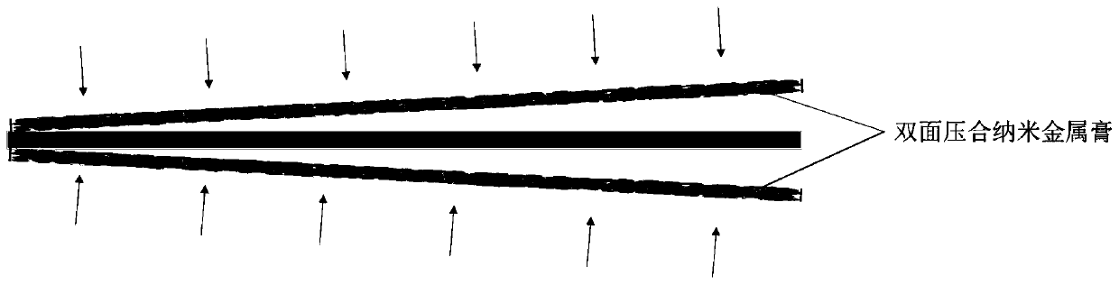
[0027] Such as Figure 4 As shown, it is a schematic diagram of the new graphene crystal-bonding material, including a Ag@Cu core-shell structure nano-metal paste film with a thickness of 200 μm and a heat dissipation layer with a thickness of 40 μm. The size is 50nm, and the core-shell structure nano-metal particles account for 55.5wt.% of the metal paste film structure; the nano-metal paste film evenly covers the upper and lower surfaces of the heat dissipation layer; the heat dissipation layer is composed of multi-layer graphene; the nano-metal paste film also includes 20.0 wt.% oleic acid oxidizer, and 3.0 wt.% citric acid flux, polyvinylpyrrolidone stabilizer, activator mixture.

[0028] In a preferred embodiment, the Ag@Cu core-shell structure Ag particle size is 50nm, the Cu particle size is 10nm, the core-shell structure nano-metal particles account for 65wt.% of the metal paste f...

Embodiment 2

[0030] Embodiment 2 This embodiment provides a new type of graphene paste crystal-bonding material

[0031] The new graphene paste crystal-bonding material includes a Ni@Cu core-shell structure nano-metal paste film with a thickness of 400 μm and a heat dissipation layer with a thickness of 30 μm. The Ag@Cu core-shell structure Ag particle size is 400 nm, and the Cu particle size is 100 nm. Nano-metal particles with shell structure account for 85.5wt.% of the metal paste film structure; the nano-metal paste film evenly covers the upper and lower surfaces of the heat dissipation layer; the heat dissipation layer is composed of mixed graphene paste, and the nano-metal paste film also includes 10.0wt.% Ethanolamine oxidizer, and 3.0 wt.% lactic acid flux, polyvinylpyrrolidone stabilizer, activator mixture.

[0032] In a preferred embodiment, the Ag@Cu core-shell structure Ag particle size is 50nm, the Cu particle size is 10nm, the core-shell structure nano-metal particles account...


PUM

PropertyMeasurementUnit
thicknessaaaaaaaaaa
thicknessaaaaaaaaaa
melting pointaaaaaaaaaa

Abstract

The invention discloses a novel die bonding material and a packaging structure, and the die bonding material comprises a nano metal paste film and a heat dissipation layer, wherein the nano metal paste film uniformly covers at least one of the upper surface and the lower surface of the heat dissipation layer; the heat dissipation layer is of a multi-layer graphene structure, and the nano metal paste film comprises nano metal particles, an antioxidant, soldering flux, a stabilizer and an active agent; the content of the nano metal particles is 50.0 wt.%-95.0 wt.%, the content of the antioxidantis 5.0 wt.%-40.0 wt.%, and the total amount of the scaling powder, the stabilizer and the active agent is less than or equal to 5.0 wt.%. The material has the characteristics of high heat dissipationand uniform thickness; on the premise that the electrical performance of the semiconductor packaging interconnection module is not affected, die bonding and interconnection under the low-temperaturecondition are achieved, the semiconductor packaging interconnection module can be used under the conditions of small spacing, high power, high temperature, high pressure and the like, and the semiconductor packaging interconnection module can be widely applied to the fields of power electronics, IGBT packaging, photoelectron packaging, MEMS packaging, microelectronics, high-power LED packaging andthe like.

Description

technical field [0001] The invention belongs to the technical field of third-generation semiconductor packaging, and in particular relates to a novel crystal-bonding material and a packaging structure thereof. Background technique [0002] Electronic interconnection materials and interconnection substrates are the hubs of semiconductor device manufacturing, microelectronic packaging, and power electronic packaging micro-device module connection components. As representative die-bonding and interconnection substrates in the modern electronics industry, traditional interconnection substrates are mostly used It is made of electroplated copper on the surface of the plate. However, in recent years, microelectronic systems have developed towards high power, high-density integration, miniaturization, and multi-functionalization, and their production costs have been continuously reduced. Higher requirements are imposed, such as realizing high-temperature resistant interconnection (...

Claims


Application Information

Patent Timeline
Patent Type & Authority Applications(China)
IPC IPC(8): H01L23/373H01L23/52H01L23/538B82Y30/00
CPCH01L23/373H01L23/3735H01L23/3736H01L23/3733H01L23/538H01L23/52B82Y30/00
Inventor 崔成强杨斌叶怀宇张国旗
Owner SOUTH UNIVERSITY OF SCIENCE AND TECHNOLOGY OF CHINA
Why Eureka
Try Eureka