GaN junction field effect transistor device with core-shell structure and preparation method of device
A field-effect transistor and core-shell technology, which is used in semiconductor/solid-state device manufacturing, semiconductor devices, electrical components, etc., can solve problems such as complex preparation processes, and achieve the effects of good electric field uniformity, strong control ability, and improved reliability.
- Summary
- Abstract
- Description
- Claims
- Application Information
AI Technical Summary
Problems solved by technology
Method used
Image

Examples
Embodiment 1
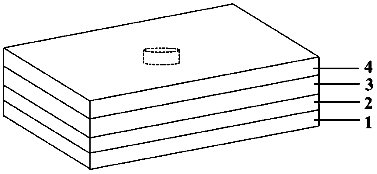
[0040] Such as Figure 1-4 Shown, a kind of preparation method of core-shell structure GaN-JFET device, its step comprises:
[0041] (1) MOCVD method deposits semi-insulating GaN layer 2 and the first heavily doped n-GaN layer 3 on the surface of sapphire substrate 1, as figure 1 Shown; growth method of semi-insulating GaN: trimethylgallium and NH 3 As Ga source and N source respectively, the carrier gas is H 2 or N 2 , the growth temperature is 1000-1100°C, and the growth time is 3-5h. Growth method of heavily doped n-GaN layer: temperature 950-1050°C, silicon doping concentration 1*1019 cm -3 , growth time 25-30min. Growth of patterned Si on heavily doped n-GaN layer by PECVD and photolithography 3 N 4 Mask layer 4, Si grown after patterning by photolithography 3 N 4 Regular holes are formed on the membrane, and n-GaN nanocolumns are grown in the holes by MBE;
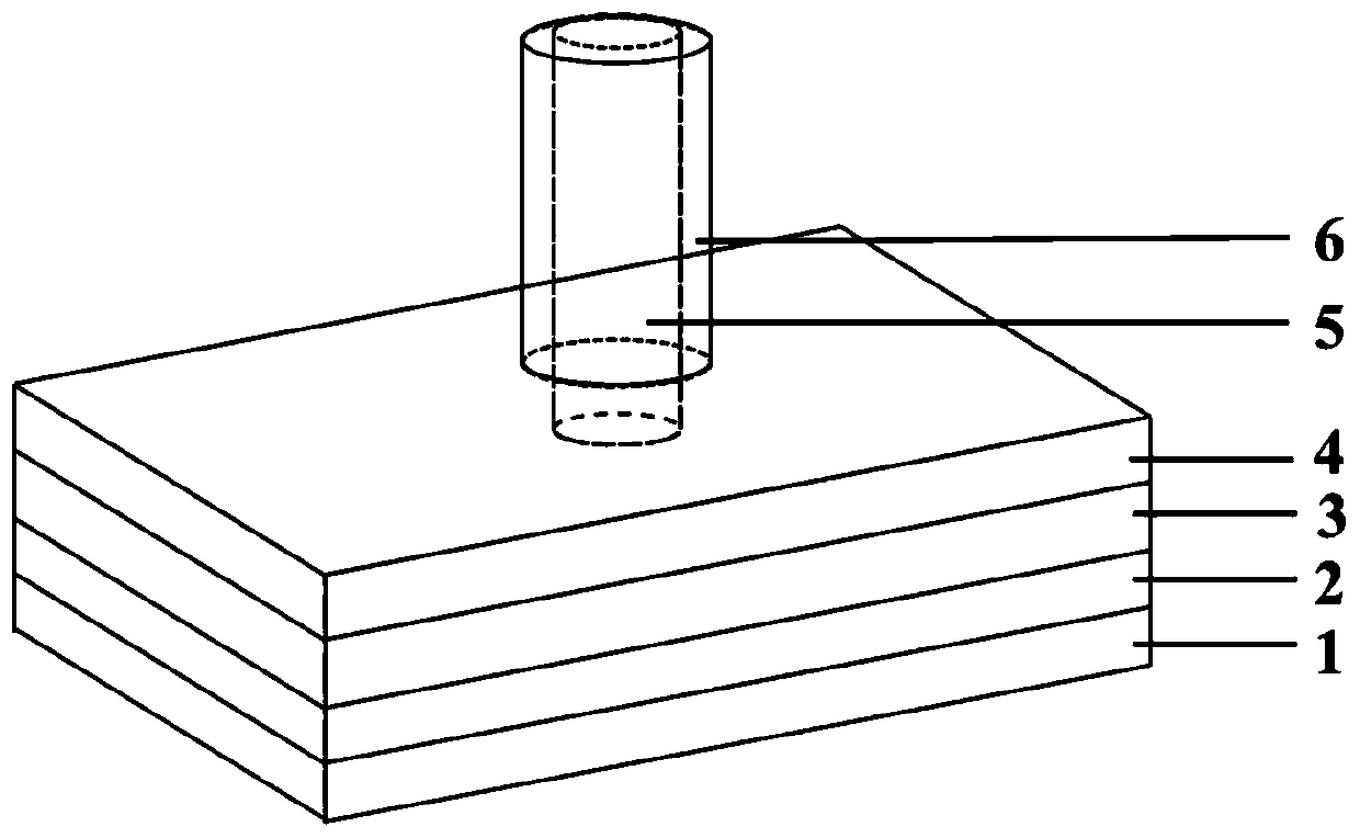
[0042] (2) MBE method on the first heavily doped n-GaN layer, Si 3 N 4 The epitaxial core-shell nano-c...
Embodiment 2
[0046] The core-shell structure GaN-JFET device, its structure includes:
[0047] A sapphire substrate layer;
[0048] A semi-insulating GaN layer grown on the substrate layer with a thickness of 2 μm;
[0049] A first heavily doped n-GaN layer grown on the semi-insulating GaN layer with a thickness of 300nm, patterned Si grown on the heavily doped n-GaN layer 3 N 4 Layer, the thickness of which is 100nm, the n-GaN nanocolumn channel layer grown on the first heavily doped n-GaN layer, the diameter is 200nm, the height is 800nm, and the n-GaN silicon doping concentration is 1*10 18 cm -3 , the p-GaN nano ring grown on the outside of the n-GaN nano column channel layer, p-GaN and n-GaN channel layer form a core-shell p-n junction, p-GaN thickness 150nm, height 600nm, p- The doping concentration of GaN is 1*10 18 cm -3 ;
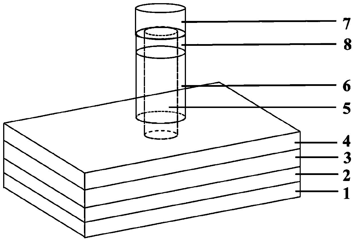
[0050] It also includes a second heavily doped n-GaN layer on the channel of the n-GaN nanocolumn, the thickness of which is 300nm, and Si between the s...
Embodiment 3
[0054] The core-shell structure GaN junction field effect transistor device, its structure includes:
[0055] a SiC substrate layer;
[0056] A semi-insulating GaN layer grown on the substrate layer with a thickness of 5 μm;
[0057] A first heavily doped n-GaN layer grown on the semi-insulating GaN layer with a thickness of 300nm, patterned Si grown on the heavily doped n-GaN layer 3 N 4 Layer, the thickness of which is 100nm, the n-GaN nanocolumn channel layer grown on the first heavily doped n-GaN layer, the diameter is 200nm, the height is 800nm, and the n-GaN silicon doping concentration is 1*10 18 cm -3 , the p-GaN nano ring grown on the outside of the n-GaN nano column channel layer, p-GaN and n-GaN channel layer form a core-shell p-n junction, p-GaN thickness 150nm, height 600nm, p- The doping concentration of GaN is 1*10 18 cm -3 ;
[0058] It also includes a second heavily doped n-GaN layer on the channel of the n-GaN nanocolumn, the thickness of which is 300n...
PUM
| Property | Measurement | Unit |
|---|---|---|
| Height | aaaaa | aaaaa |
| Layer thickness | aaaaa | aaaaa |
| Thickness | aaaaa | aaaaa |
Abstract
Description
Claims
Application Information
 - R&D
- Intellectual Property
- Life Sciences
- Materials
- Tech Scout
- Unparalleled Data Quality
- Higher Quality Content
- 60% Fewer Hallucinations
Browse by: Latest US Patents, China's latest patents, Technical Efficacy Thesaurus, Application Domain, Technology Topic, Popular Technical Reports.
© 2025 PatSnap. All rights reserved.Legal|Privacy policy|Modern Slavery Act Transparency Statement|Sitemap|About US| Contact US: help@patsnap.com