MOS structure trench diode device and manufacturing method thereof

A technology of MOS structure and manufacturing method, which is applied in semiconductor/solid-state device manufacturing, semiconductor devices, electrical components, etc., can solve the problems of low forward voltage and inability to achieve low and high temperature leakage characteristics, and achieve the concentration and realization of weakened electric field The effect of cutting off surface channel leakage and reducing the requirements of photolithography process

Active Publication Date: 2020-07-14
江苏新顺微电子股份有限公司
View PDF4 Cites 3 Cited by
  • Summary
  • Abstract
  • Description
  • Claims
  • Application Information

AI Technical Summary

Problems solved by technology

[0004] Aiming at the problems existing in the prior art, the present invention provides a MOS structure trench diode device to solve the characteristic technical problem of not being able to achieve both low and high temperature leakage characteristics and low forward voltage

Method used


Image

  • MOS structure trench diode device and manufacturing method thereof
  • MOS structure trench diode device and manufacturing method thereof
  • MOS structure trench diode device and manufacturing method thereof

Examples


specific Embodiment 1

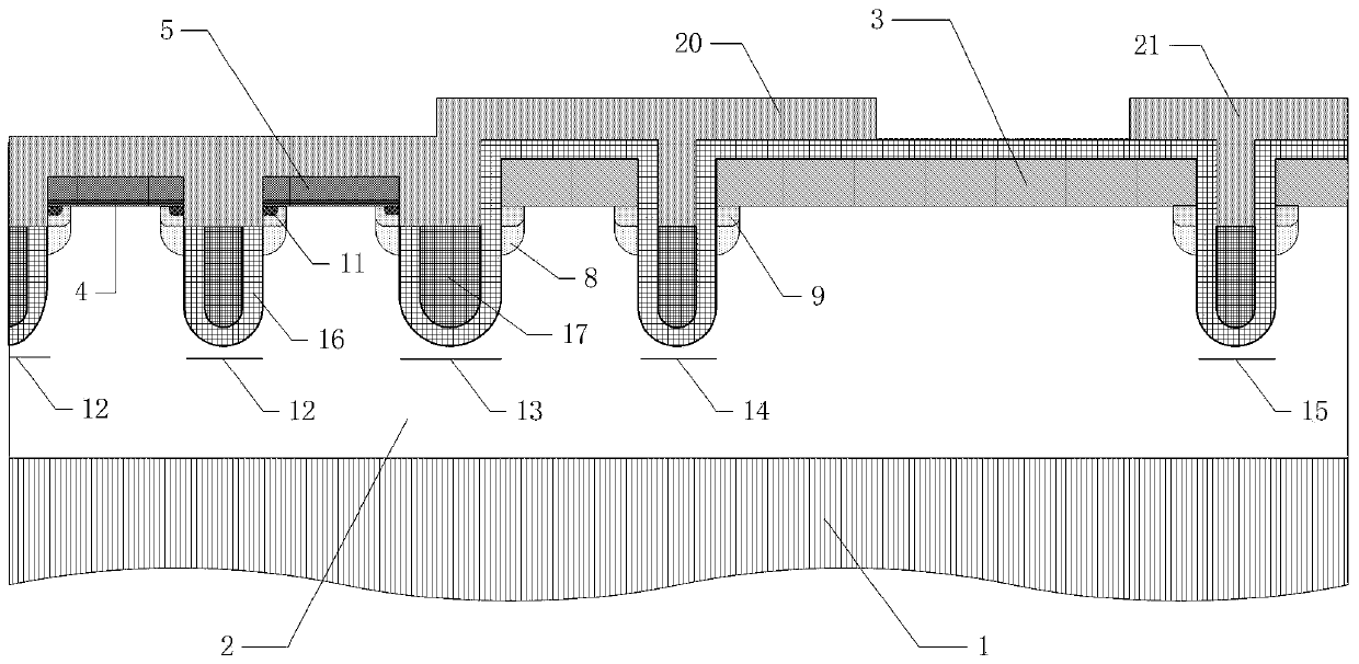
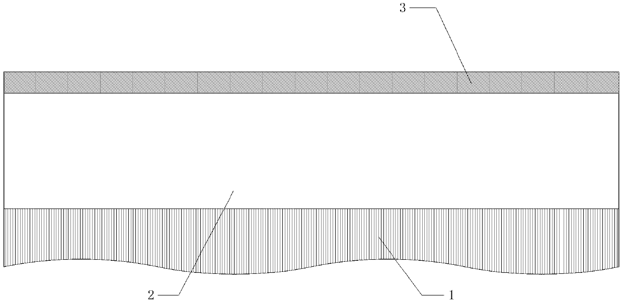
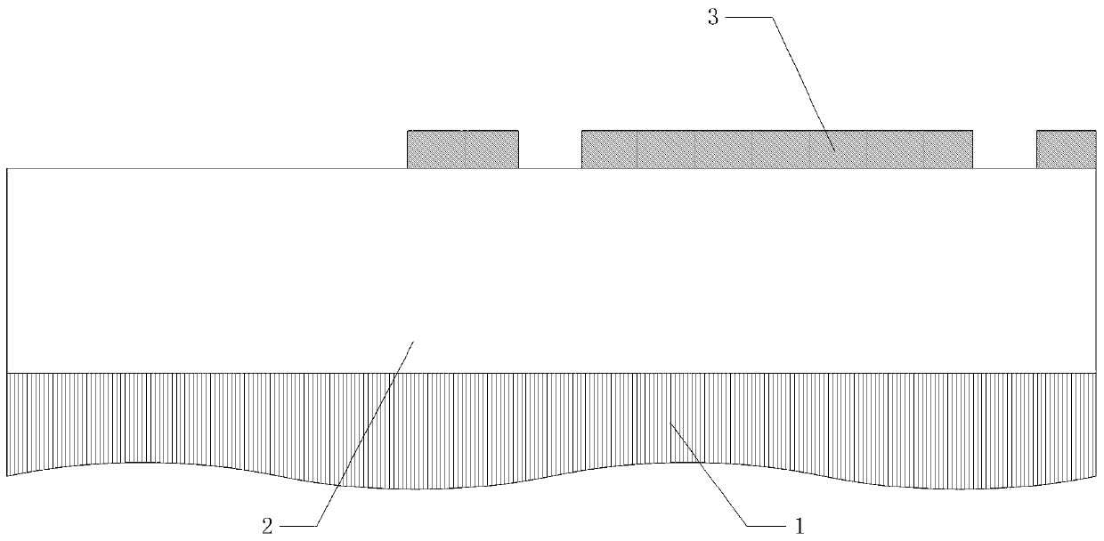
[0088] Specific embodiment 1, see figure 1 , a trench diode device with a MOS structure, comprising a silicon substrate 1 of the first conductivity type and an epitaxial layer 2 of the first conductivity type arranged in sequence from bottom to top, and on the epitaxial layer 2 are arranged sequentially from left to right at least Two original cell grooves 12, a large original cell groove 13, an extension groove 14 and a stop groove 15, the width of the original cell groove 12 is less than the width of the original cell large groove 13; the original cell groove 12, the original cell The inner walls of the large trench 13, the extended trench 14 and the cut-off trench 15 are sequentially provided with a silicon dioxide outer layer 16 and a polysilicon filling layer 17;

[0089] On the epitaxial layer 2, a gate oxide layer 4 (that is, SiO 2 layer), a polysilicon layer 5 of the first conductivity type is provided above the gate oxide layer 4;

[0090] The first doped region 8 a...


PUM

PropertyMeasurementUnit
depthaaaaaaaaaa
widthaaaaaaaaaa
thicknessaaaaaaaaaa

Abstract

The invention discloses an MOS structure trench diode device and a manufacturing method thereof. The MOS structure trench diode device comprises a silicon substrate and an epitaxial layer which are sequentially arranged from bottom to top, wherein a primitive cell trench, a primitive cell large trench, an extension trench and a cut-off trench which are sequentially arranged are formed in the epitaxial layer; the inner side walls of the primitive cell trench, the primitive cell large trench, the extension trench and the cut-off trench are sequentially provided with a silicon dioxide outer layerand a polycrystalline silicon filling layer; a gate oxide layer is arranged in an area between two adjacent primitive cell grooves on the epitaxial layer, and a polycrystalline silicon layer is arranged above the gate oxide layer; first doped regions and second doped regions are arranged on the left sides and the right sides of the tops of the primitive cell groove, the primitive cell large groove, the extension groove and the cut-off groove; third doped regions are arranged on the left side and the right side of the top of the primitive cell groove and the side, close to the primitive cell groove, of the primitive cell large groove. The device also includes a first metal layer and a second metal layer arranged on the left side and the right side. By introducing the voltage division and electric field shielding effects of the trench MOS, the performance of the device is improved, and the application field is broadened.

Description

technical field [0001] The invention relates to the technical field of semiconductors, in particular to a diode device and a manufacturing method thereof. Background technique [0002] The diode device with MOS structure is a relatively new type of low power consumption diode rectifier device, which has a lower forward voltage drop than ordinary PN junction diodes; compared with ordinary Schottky diodes, it has a higher Low high temperature reverse leakage, so it is more suitable for some applications that require lower forward voltage drop and lower high temperature reverse leakage. [0003] However, the existing MOS structure diode devices also have shortcomings. Similar to the electrical characteristics of Schottky diodes, their reverse leakage and forward voltage drop are also a pair of contradictory parameters, and as the temperature increases, the leakage of all diodes They are all rising; after achieving balance, its comprehensive performance is not as good as that o...

Claims


Application Information

Patent Timeline
Patent Type & Authority Applications(China)
IPC IPC(8): H01L29/872H01L29/06H01L21/329
CPCH01L29/0688H01L29/6609H01L29/8725
Inventor 陈晓伦韩笑朱涛鞠柯孟军徐励远
Owner 江苏新顺微电子股份有限公司
Why Eureka
Try Eureka