Metal interconnection structure and preparation method thereof

A metal interconnection structure and metal pattern technology, which is applied in semiconductor/solid-state device manufacturing, electrical components, electric solid-state devices, etc., can solve problems such as unfavorable line patterns, overhanging protrusions, and inability to form line patterns in grooves to achieve high flow and recrystallization ability, the effect of avoiding the increase of defective rate

Pending Publication Date: 2020-07-28
XIA TAI XIN SEMICON QING DAO LTD
View PDF5 Cites 0 Cited by
  • Summary
  • Abstract
  • Description
  • Claims
  • Application Information

AI Technical Summary

Problems solved by technology

However, due to the small size of the semiconductor device, it is easy to cause when the seed layer cannot be uniformly deposited on the inner surface of the trench, so that the phenomenon of overhang (Overhang) appears on the top of the trench, which is not conducive to the formation of subsequent circuit patterns.
Even, when the overhanging phenomenon is more serious, the top of the trench will be completely sealed, resulting in the inability to form a circuit pattern inside the trench

Method used


Image

  • Metal interconnection structure and preparation method thereof
  • Metal interconnection structure and preparation method thereof
  • Metal interconnection structure and preparation method thereof

Examples


Embodiment Construction

[0031] The present invention will be further described below in conjunction with the accompanying drawings and embodiments.

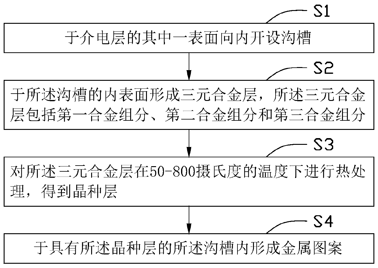
[0032] see figure 1 , the embodiment of the present invention provides a method for preparing a metal interconnection structure 100, including the following steps:

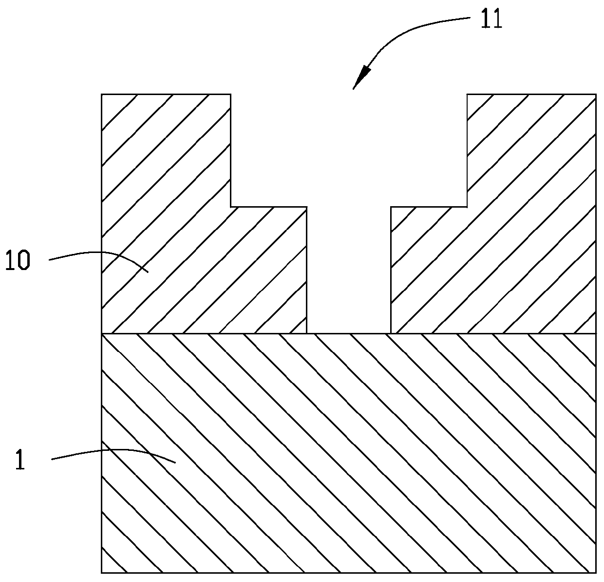
[0033] Step S1, see figure 2 A trench 11 is opened inwardly on one of the surfaces of the dielectric layer 10 .

[0034] In this embodiment, the trench 11 can be obtained by covering the surface of the dielectric layer 10 with a patterned photoresist (not shown in the figure) and performing etching.

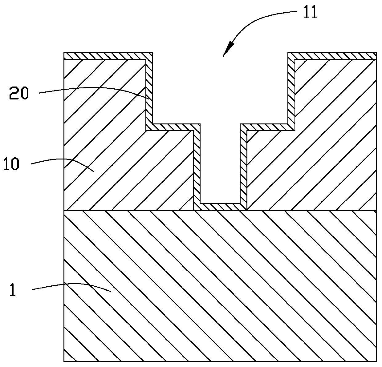
[0035] Further, as image 3 As shown, after opening the trench 11 , a diffusion barrier layer 20 is formed at least on the inner surface of the trench 11 (including the sidewall and the bottom surface of the trench 11 ). The diffusion barrier layer 20 may include one of tantalum, titanium, manganese, tantalum nitride, titanium nitride and manganese nitride.

[0036] In this embodiment, t...


PUM


Abstract

The invention provides a metal interconnection structure and a preparation method thereof. The method comprises the steps of forming a groove inwards in one surface of a dielectric layer; forming a ternary alloy layer in the groove, wherein the ternary alloy layer comprises a first alloy component, a second alloy component and a third alloy component, the first alloy component is copper, the second alloy component is manganese, the third alloy component is one of silver, titanium, chromium, cobalt, nickel, zirconium, yttrium, ruthenium, rhodium, palladium, cadmium, iridium, platinum, gold, aluminum, magnesium and selenium, the atom percentage content of the second alloy component in the ternary alloy layer is 0-15%, and the atom percentage content of the third alloy component in the ternary alloy layer is 6-15%; and the ternary alloy layer is subjected to heat treatment at the temperature of 50-800 DEG C to obtain a seed crystal layer.

Description

technical field [0001] The invention relates to the field of semiconductors, in particular to a metal interconnection structure and a preparation method thereof. Background technique [0002] As the size of semiconductor devices is gradually miniaturized, the size of circuit patterns of integrated circuits formed on semiconductor devices is also developing toward miniaturization. Existing studies have shown that in order to suppress copper diffusion in integrated circuits, it is usually necessary to deposit a copper-manganese alloy seed layer by a physical vapor deposition (Physical Vapor Deposition; PVD) process before forming circuit patterns. However, due to the small size of the semiconductor device, when the seed layer cannot be uniformly deposited on the inner surface of the trench, an overhang phenomenon occurs on the top of the trench, which is not conducive to the formation of subsequent circuit patterns. Even, when the overhanging phenomenon is more severe, the to...

Claims


Application Information

Patent Timeline
Patent Type & Authority Applications(China)
IPC IPC(8): H01L21/768H01L23/532
CPCH01L21/76873H01L21/76843H01L21/76864H01L23/53238
Inventor 金志勲金玄永徐康元
Owner XIA TAI XIN SEMICON QING DAO LTD
Why Eureka
Try Eureka