Method for preparing graphene-based transistor and channel material thereof through electro-deposition
A graphene-based, transistor technology, applied in electrolytic coatings, metal material coating processes, circuits, etc., can solve problems such as difficult repetition, high cost, and difficult operation.
- Summary
- Abstract
- Description
- Claims
- Application Information
AI Technical Summary
Problems solved by technology
Method used
Image

Examples
Embodiment 1
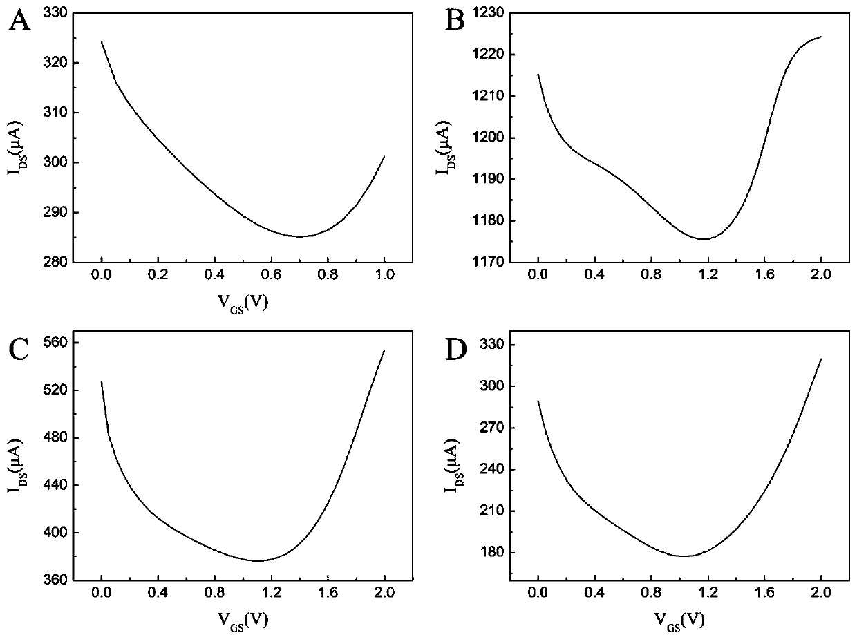
[0025] Electrodeposition prepares the graphene-based transistor channel material and the method for preparing the graphene-based transistor, the steps of which are as follows:
[0026] The first step is to plate gold and chromium on a 1x1cm glass substrate by evaporation coating method. The thickness of chromium is controlled at about 0.3-1nm, and the thickness of gold is controlled at about 30-100nm, which are used as the gate and source of the transistor , Drain, the distance between source and drain is 250μm;
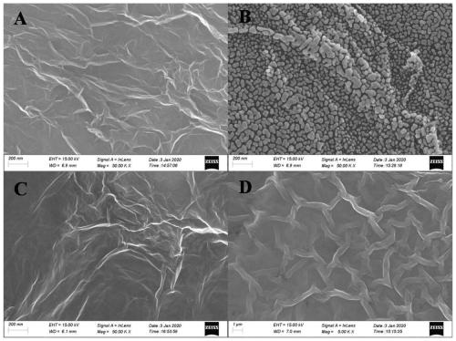
[0027] In the second step, use adhesive tape to fix a size of 5 mm × 5 mm in the channel, disperse graphene oxide in ultrapure water for 1 hour, and then drop-coat it on the fixed channel. The concentration of graphene oxide is 0.5 mg / mL. After drying, the channel region of the transistor is modified with graphene oxide;
[0028] The third step, 1. Use the electrochemical workstation to set the scanning speed of cyclic voltammetry to 50mV / s, and the number of scanni...
Embodiment 2
[0034] Electrodeposition prepares the graphene-based transistor channel material and the method for preparing the graphene-based transistor, the steps of which are as follows:
[0035] The first step is to plate gold and chromium on a 1x1cm glass substrate by evaporation coating method. The thickness of chromium is controlled at about 0.3-1nm, and the thickness of gold is controlled at about 30-100nm, which are used as the gate and source of the transistor , Drain, the distance between source and drain is 100μm;
[0036] In the second step, use adhesive tape to fix the size of 5mm×5mm in the channel, disperse graphene oxide in ultrapure water for 1h, and then drop-coat it on the fixed channel. The concentration of graphene oxide is 0.8mg / mL, and the After drying, the channel region of the transistor is modified with graphene oxide;
[0037] The third step, 1. Use the electrochemical workstation to set the scanning speed of cyclic voltammetry to 50mV / s, and the number of scann...
Embodiment 3
[0041] Electrodeposition prepares the graphene-based transistor channel material and the method for preparing the graphene-based transistor, the steps of which are as follows:
[0042] The first step is to plate gold and chromium on a 1x1cm glass substrate by evaporation coating method. The thickness of chromium is controlled at about 0.3-1nm, and the thickness of gold is controlled at about 30-100nm, which are used as the gate and source of the transistor , Drain, the distance between source and drain is 250μm;
[0043] In the second step, use adhesive tape to fix the size of 5mm×5mm in the channel, disperse graphene oxide in ultrapure water for 1h, and then drop-coat it on the fixed channel. The concentration of graphene oxide is 0.3mg / mL, and the After drying, the channel region of the transistor is modified with graphene oxide;
[0044] The third step, 1. Use the electrochemical workstation to set the scanning speed of cyclic voltammetry to 50mV / s, and the number of scann...
PUM
 Abstract
Description
Claims
Application Information
 - R&D
- Intellectual Property
- Life Sciences
- Materials
- Tech Scout
- Unparalleled Data Quality
- Higher Quality Content
- 60% Fewer Hallucinations
Browse by: Latest US Patents, China's latest patents, Technical Efficacy Thesaurus, Application Domain, Technology Topic, Popular Technical Reports.
© 2025 PatSnap. All rights reserved.Legal|Privacy policy|Modern Slavery Act Transparency Statement|Sitemap|About US| Contact US: help@patsnap.com