Method for manufacturing ultra-small magnetic random access memory array

A random access memory, ultra-small technology, applied in the fields of magnetic field-controlled resistors, electric solid-state devices, semiconductor devices, etc., can solve the problems of reduced sidewall trimming efficiency, difficult sidewall damage, etc., to improve trimming efficiency and reduce shadows effect, reducing the effect of redeposition

Active Publication Date: 2020-08-04
SHANGHAI CIYU INFORMATION TECH CO LTD
View PDF14 Cites 1 Cited by
  • Summary
  • Abstract
  • Description
  • Claims
  • Application Information

AI Technical Summary

Problems solved by technology

[0008] Patent: US 2018 / 0190901A1 provides a method to prevent the short circuit between the magnetic tunnel junction reference layer and the memory layer, specifically: deposit a layer of insulating material at the front end of the etching of the bottom electrode of the magnetic tunnel junction to reduce the subsequent trimming of the sidewall At the same time, the by-products brought about by the etching front end are deposited again. However, with this method, when depositing the insulating layer, a thicker insulating layer will also be deposited around the hard mask and the magnetic tunnel junction. With the existence of the insulating layer, the efficiency of sidewall trimming will be greatly reduced or it will be difficult to remove the sidewall damage / deposition layer

Method used


Image

  • Method for manufacturing ultra-small magnetic random access memory array
  • Method for manufacturing ultra-small magnetic random access memory array
  • Method for manufacturing ultra-small magnetic random access memory array

Examples


Embodiment 1

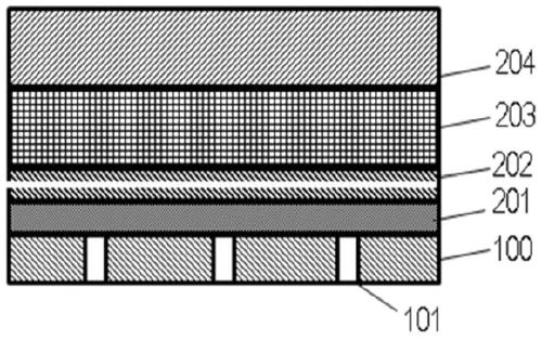
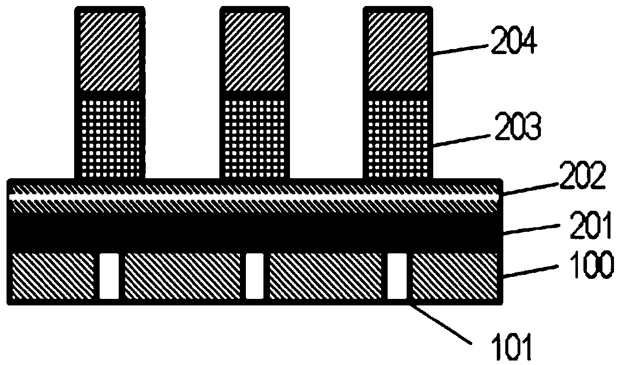
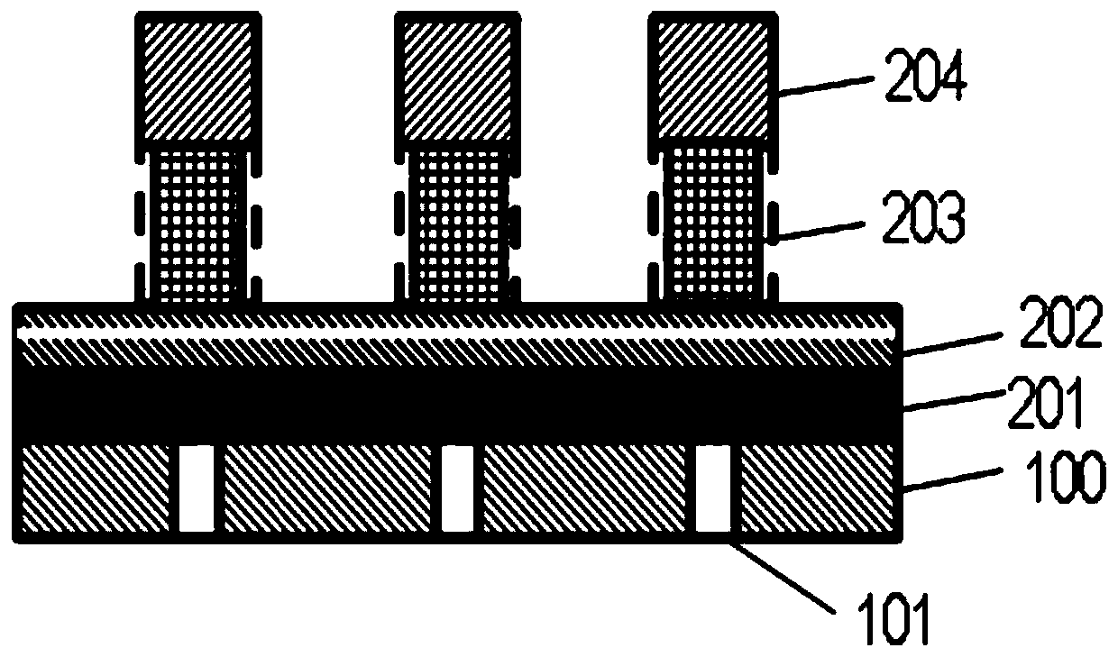
[0051] Step 1, such as figure 1 As shown, a substrate 100 with a surface-polished CMOS VIA101 is provided, and a bottom electrode 201 , a magnetic tunnel junction 202 of a multilayer film structure, a film layer of a hard mask 203 and a film layer of a sacrificial mask 204 are deposited on the substrate.

[0052] Among them, the thickness of the bottom electrode is 5nm-80nm, and its constituent materials are Ti, TiN, Ta, TaN, W, WN or any combination thereof, generally using physical vapor deposition (Physical Vapor Deposition, PVD), usually after deposition, Chemical-mechanical polishing is performed on it to achieve surface flatness for making magnetic tunnel junctions.

[0053] The multilayer film thickness of the magnetic tunnel junction (MTJ) 202 is 8nm-40nm, which can be a bottom pinned (Bottom Pinned) structure consisting of a reference layer, a barrier layer and a memory layer stacked upwards in sequence, or a memory layer, a barrier layer Layers and reference layers ...


PUM

PropertyMeasurementUnit
thicknessaaaaaaaaaa
thicknessaaaaaaaaaa
thicknessaaaaaaaaaa

Abstract

The invention provides a method for manufacturing an ultra-small magnetic random access memory array. The method comprises the following steps: depositing a bottom electrode, a magnetic tunnel junction (MTJ), a hard mask and sacrificial mask layers on a substrate; graphically defining an MTJ pattern, and selectively and laterally demagnifying the hard mask and the sacrificial mask; etching the MTJuntil reaching the bottom electrode and maintaining a small amount of over-etching; depositing insulating layers, and enabling the thickness of the insulating layer on the bottom electrode etching front end and the sacrificial mask top to be greater than the thickness of the insulating layer on the side walls of the MTJ and the hard mask; trimming the side walls of the MTJ; depositing a self-aligning mask for etching the bottom electrode; etching the bottom electrode; and covering an insulating covering layer, and filling the dielectric and grinding the dielectric. According to the method, two times of etching are adopted when the MTJ and the bottom electrode are etched, so that the shadow effect is effectively reduced; and in addition, after the hard mask is etched, the transverse trimming process is added, so that the thickness of insulating layers deposited at the subsequent bottom electrode etching front end and the top end of the sacrificial mask is larger than the thickness of insulating layers deposited on the side walls of the MTJ and the side walls of the hard mask, and trimming efficiency is greatly improved.

Description

technical field [0001] The invention relates to the technical field of semiconductor chip manufacturing, in particular to a method for manufacturing an ultra-small magnetic random access memory unit array. Background technique [0002] In recent years, Magnetic Random Access Memory (MRAM) using Magnetic Tunnel Junction (Magnetic Tunnel Junction, MTJ) is considered to be the future solid-state non-volatile memory, which has high-speed reading and writing, large capacity and low energy consumption. consumption characteristics. Ferromagnetic MTJ is usually a sandwich structure, which has a magnetic memory layer, which can change the magnetization direction to record different data; an insulating tunnel barrier layer in the middle; a magnetic reference layer, located on the other side of the tunnel barrier layer, which The direction of magnetization remains unchanged. [0003] In order to record information in this magnetoresistive element, it is suggested to use a writing met...

Claims


Application Information

Patent Timeline
Patent Type & Authority Applications(China)
IPC IPC(8): H01L43/08H01L43/12H01L27/22
CPCH10B61/22H10N50/01H10N50/10Y02D10/00
Inventor 张云森郭一民陈峻肖荣福
Owner SHANGHAI CIYU INFORMATION TECH CO LTD
Why Eureka
Try Eureka