Receiving device based on waveguide balance detector and integration method thereof

A technology for a balanced detector and a receiving device, applied in the field of balanced detection, can solve the problems of complex optical path setting method, small detection field of view, poor integration, etc., and achieves the effects of low adjustment difficulty, small volume, and small light loss.

Active Publication Date: 2020-08-07
INFORMATION SCI RES INST OF CETC
View PDF5 Cites 6 Cited by
  • Summary
  • Abstract
  • Description
  • Claims
  • Application Information

AI Technical Summary

Problems solved by technology

[0004] The present invention proposes a receiving device and an integration method based on a waveguide balanced detector, aiming to solve the problem that the existing balanced detector receiving

Method used


Image

  • Receiving device based on waveguide balance detector and integration method thereof
  • Receiving device based on waveguide balance detector and integration method thereof
  • Receiving device based on waveguide balance detector and integration method thereof

Examples


Embodiment 1

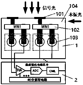
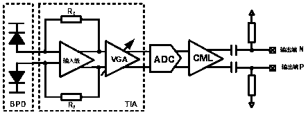
[0042] figure 1 A schematic structural diagram of a receiving device based on a waveguide balanced detector according to an embodiment of the present application is shown in . figure 2 A schematic diagram of a circuit principle of a receiving device based on a waveguide balanced detector according to an embodiment of the present application is shown in .

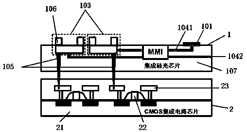
[0043] Such as figure 1 As shown, the receiving device based on the waveguide balanced detector provided in the embodiment of the present application includes an integrated silicon photonic chip 1 and a readout circuit chip 2. In the receiving device based on the waveguide balanced detector in this embodiment, the integrated silicon photonic chip 1 includes a passive silicon optical device and an active waveguide balance detector 103, and the integrated silicon optical chip 1 and the readout circuit chip 2 are interconnected in a three-dimensional stacked manner through silicon vias, that is, through-silicon-vias (through-...

Embodiment 2

[0083] This embodiment provides a method for integrating a receiving device based on a waveguide balanced detector. For details not disclosed in the receiving device and method based on a waveguide balanced detector in this embodiment, please refer to the waveguide balanced detector based on other embodiments. A detector receiving device and method.

[0084] Figure 5 A schematic diagram showing steps of an integration method of a receiving device based on a waveguide balanced detector according to an embodiment of the present application.

[0085] Such as Figure 5 As shown, the integrated method of the receiving device based on the waveguide balanced detector specifically includes the following steps:

[0086] S1: Using GeSi silicon photonics technology to integrate passive silicon photonic devices and active waveguide balance detectors to obtain integrated silicon photonic chips; using CMOS technology to integrate readout circuit chips;

[0087] S2: The integrated silico...

Embodiment 3

[0099] This embodiment provides a receiving method based on a waveguide balanced detector. For details not disclosed in the receiving device based on a waveguide balanced detector in this embodiment, please refer to the receiving device based on a waveguide balanced detector in other embodiments and integration methods.

[0100] Figure 6 A schematic diagram of steps of a receiving method based on a waveguide balanced detector according to an embodiment of the present application is shown.

[0101] Such as Figure 6 As shown, the receiving method based on the waveguide balanced detector specifically includes the following steps:

[0102] S101: receiving space signal light and local oscillator light, and obtaining a set of differential photocurrent signals through photoelectric conversion;

[0103] S102: Convert the differential photocurrent signal into a digital voltage signal.

[0104] Specifically, the spatial signal light and the local oscillator light are received thro...


PUM


Abstract

The embodiment of the invention provides a receiving device based on a waveguide balance detector and an integration method thereof, and the device comprises: an integrated silicon optical chip whichis used for receiving space signal light and local oscillation light, and obtaining a group of differential optical current signals through photoelectric conversion; a reading circuit chip which is used for converting the differential optical current signal into a digital voltage signal; and an integrated silicon optical chip which comprises a passive silicon optical device and an active waveguidebalance detector, wherein the integrated silicon optical chip and the readout circuit chip are interconnected and integrated in a three-dimensional stacking mode through silicon through holes. The receiving device based on the waveguide balance detector has the advantages of being high in integration degree, high in detection sensitivity, high in signal-to-noise ratio, capable of being expanded to a large view field and the like, three-dimensional integration of the integrated silicon optical chip and the CMOS integrated reading circuit chip is achieved through the silicon through hole technology, the size is small, the structure is simple, optical loss is small, and adjustment difficulty is low.

Description

technical field [0001] The present application belongs to the technical field of balanced detection, and in particular relates to a receiving device and an integration method based on a waveguide balanced detector. Background technique [0002] Compared with the traditional lidar ranging system, the coherent detection lidar technology based on the balanced detector not only has the advantages of strong detection ability, high conversion gain, good filtering performance, and high stability, but also has strong anti-interference ability, which can It works under the condition of strong ambient light interference, and can meet the requirements of high-precision detection. In addition, it can also detect the amplitude, intensity, phase and other information of the signal. It has a good application prospect in the laser radar ranging system. [0003] The principle of coherent detection based on balanced detectors is to place a group of photodetection devices with the same photoel...

Claims


Application Information

Patent Timeline
IPC IPC(8): H01L25/18H01L27/144H01L21/60G01S7/48
CPCG01S7/48H01L24/82H01L25/18H01L27/1443
Inventor 曹静胡小燕杨丽君李斌赵少宇王伟平郭于鹤洋
Owner INFORMATION SCI RES INST OF CETC
Why Eureka
Try Eureka