Micro-pressure sensor chip and preparation method thereof

A micro-pressure sensor and chip technology, applied in piezoelectric/electrostrictive/magnetostrictive devices, instruments, microstructure technology, etc., can solve problems such as complex process, small temperature drift, large input impedance, etc., to improve sensitivity Effects of output, improvement of dynamic performance, and improvement of natural frequency

Active Publication Date: 2020-08-11
陕西省计量科学研究院 +1
View PDF13 Cites 0 Cited by
  • Summary
  • Abstract
  • Description
  • Claims
  • Application Information

AI Technical Summary

Problems solved by technology

[0003] Pressure sensors with different sensitivity principles have their own advantages and disadvantages: for example, piezoelectric sensors are limited by their sensitivity principles and cannot measure static pressure, and the output charge signal needs to be processed by subsequent complex auxiliary circuits; capacitive pressure sensors have high sensitivity, The temperature drift is small, the power consumption is low, but the input impedance is large, it is easily affected by the parasitic capacitance, and it is more sensitive to the interference of the surrounding environment; t

Method used


Image

  • Micro-pressure sensor chip and preparation method thereof
  • Micro-pressure sensor chip and preparation method thereof
  • Micro-pressure sensor chip and preparation method thereof

Examples


Embodiment Construction

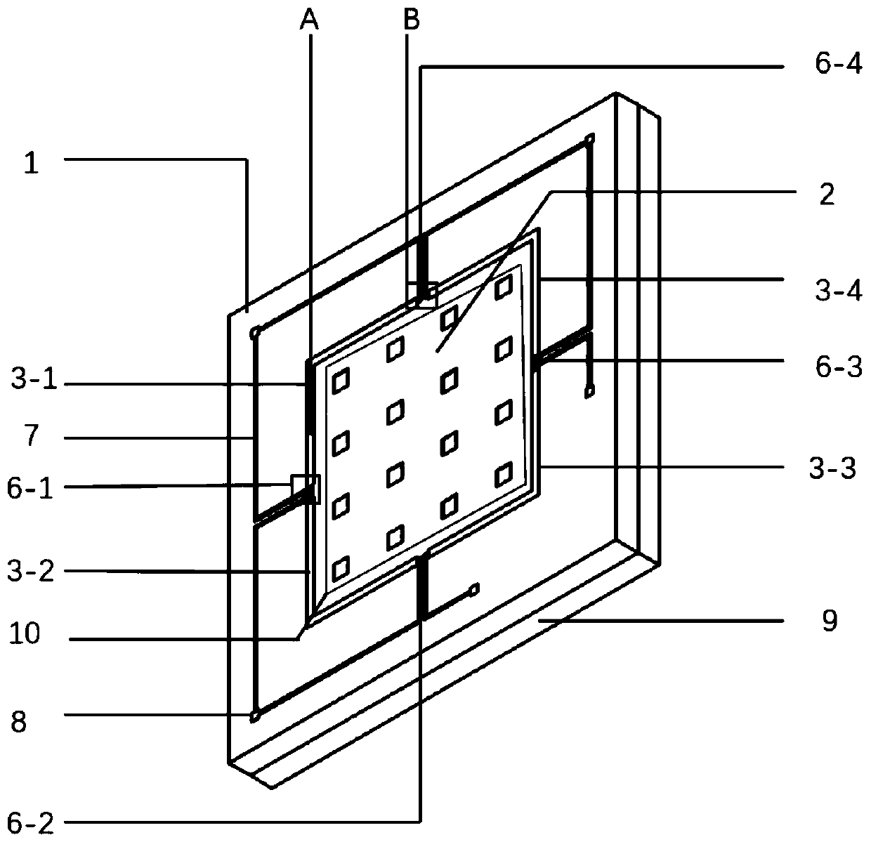
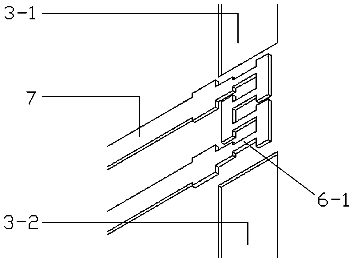
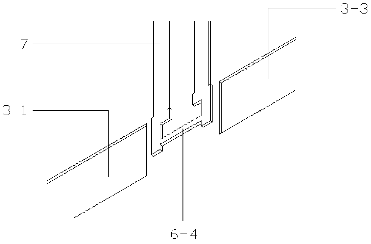
[0045] In order to make the purpose and technical solution of the present invention clearer and easier to understand. The present invention will be further described in detail below in conjunction with the drawings and embodiments. The specific embodiments described here are only used to explain the present invention, not to limit the present invention.

[0046] In describing the present invention, it should be understood that the terms "center", "longitudinal", "transverse", "upper", "lower", "front", "rear", "left", "right", " The orientations or positional relationships indicated by "vertical", "horizontal", "top", "bottom", "inner" and "outer" are based on the orientations or positional relationships shown in the drawings, and are only for the convenience of describing the present invention and Simplified descriptions, rather than indicating or implying that the device or element referred to must have a particular orientation, be constructed and operate in a particular ori...


PUM


Abstract

The invention discloses a micro-pressure sensor chip and a preparation method thereof. The sensor chip mainly comprises a stress film, a substrate, a piezoresistive strip, a metal lead, an overload protection assembly and the like. According to the specific structure, a stress film with a stress adjusting groove and a stress concentration groove is manufactured on a chip structure substrate. Fourstress concentration grooves are evenly distributed in the edge of the stress film, the four piezoresistor strips are arranged between the ends of every two adjacent stress concentration grooves, andthe piezoresistor strips are connected into a semi-open-loop Wheatstone bridge through the metal leads. The gap between the cross support beam and the bump of the chip back cavity further improves thestress concentration effect at the piezoresistor strip. The main preparation process comprises the following steps of: manufacturing a piezoresistor strip for a cleaned SOI silicon wafer, manufacturing an ohmic contact region by adopting P-type heavy doping, manufacturing a metal lead and a bonding pad, etching a stress concentration groove and a stress adjustment groove by a dry method, manufacturing a back cavity structure of a chip, and finally bonding a manufactured chip structure substrate with anti-overload glass.

Description

technical field [0001] The invention belongs to the technical field of MEMS piezoresistive micro-pressure sensors, and in particular relates to a micro-pressure sensor chip and a preparation method thereof. Background technique [0002] At present, MEMS micro-pressure sensors have been widely used in biomedical, aerospace, wind tunnel testing and other fields, especially in the aerospace field that has strict requirements on the volume, weight, sensitivity and natural frequency of the sensor. MEMS sensors are widely used due to their small size and high precision. For example, in the field of medical equipment, cardiovascular automatic testers use micro-pressure sensors as measurement sensitive elements to measure radial artery information. In order to ensure the accuracy of diagnosis, the accuracy of micro-pressure sensors Higher requirements are placed on performance and repeatability. In the field of unmanned aerial vehicles, it is of great significance to monitor the fl...

Claims


Application Information

Patent Timeline
IPC IPC(8): G01L1/20G01L9/02B81B7/02B81C1/00
CPCG01L1/20G01L9/02B81B7/02B81C1/00015B81B2201/0264
Inventor 王鸿雁赵立波吴永顺魏于昆山涛皇咪咪徐廷中陈翠兰李学琛蒋庄德
Owner 陕西省计量科学研究院
Why Eureka
Try Eureka