HEMT type ultraviolet detector with interdigital p-GaN gate structure and preparation method of HEMT type ultraviolet detector

A technology of ultraviolet detector and grid structure, applied in semiconductor/solid-state device manufacturing, semiconductor devices, electrical components, etc., can solve the problem of increasing device structure complexity and device cost, ultraviolet light loss, device photoresponsivity and other performance degradation, etc. problem, to achieve the effect of increasing the effective light-receiving area, improving the utilization rate of the sample, and increasing the optical gain

Pending Publication Date: 2020-08-11
南京冠鼎光电科技有限公司
View PDF4 Cites 1 Cited by
  • Summary
  • Abstract
  • Description
  • Claims
  • Application Information

AI Technical Summary

Problems solved by technology

This not only increases the complexity of the device structure and device cost, but also causes a certain degree of ultraviolet light loss, which reduces the performance of the device such as photoresponsivity.

Method used


Image

  • HEMT type ultraviolet detector with interdigital p-GaN gate structure and preparation method of HEMT type ultraviolet detector
  • HEMT type ultraviolet detector with interdigital p-GaN gate structure and preparation method of HEMT type ultraviolet detector
  • HEMT type ultraviolet detector with interdigital p-GaN gate structure and preparation method of HEMT type ultraviolet detector

Examples


Embodiment 1

[0036] A method for preparing an interdigitated p-GaN gate structure HEMT type ultraviolet detector, the steps comprising:

[0037] (1) Sample cleaning: Pollutants and oxides on the surface of the sample will reduce the performance of the device, so the cleaning of the sample is also a very important link in the semiconductor process. First, put the sample into acetone to dissolve the organic pollutants on the surface of the sample, then dissolve it with alcohol to remove the remaining acetone, and finally wash off the alcohol with deionized water. Soak in diluted hydrochloric acid (the volume ratio of water and hydrochloric acid is 4:1) for 10 minutes, and finally put in acetone, alcohol and deionized water for ultrasonic cleaning, dry the moisture on the surface of the sample with a nitrogen gun, and place Bake on a baking table at 100°C for 90s to dry the remaining moisture, so as to avoid its influence on the subsequent photoresist leveling.

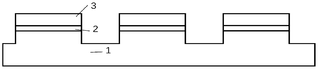
[0038](2) Etching of the iso...

Embodiment 2

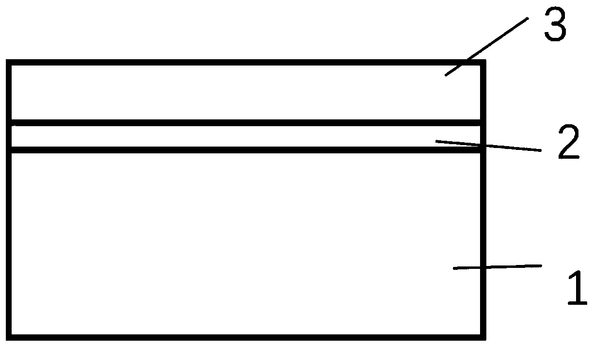
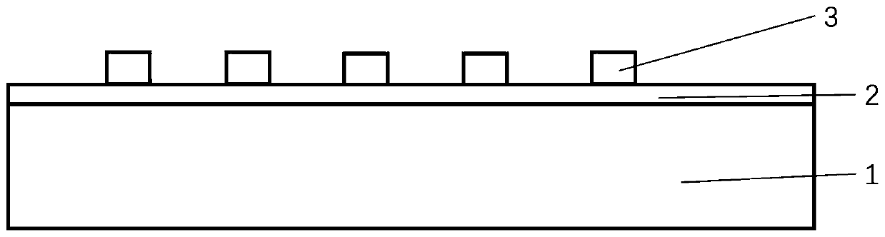
[0042] An interdigitated p-GaN gate structure HEMT type ultraviolet detector, its structure includes from bottom to top:

[0043] Sapphire substrate layer;

[0044] GaN buffer layer with a thickness of 20nm;

[0045] i-GaN layer with a thickness of 1 μm;

[0046] An unintentionally doped AlGaN layer with a thickness of 12nm and an Al composition of 20%;

[0047] p-GaN layer with a Mg doping concentration of 1×10 19 cm –3 ;

[0048] The p-GaN layer is distributed in a reciprocating zigzag pattern on the AlGaN layer, and a plurality of parallel transverse p-GaN lines are arranged on the mesa of the AlGaN layer, and all parallel p-GaN lines are connected end to end by vertical p-GaN lines , forming a complete p-GaN line, the p-GaN line divides the AlGaN layer mesa into two parts, the width of the p-GaN line is 2 μm, the thickness is 100 nm, and the distance between adjacent lateral p-GaN lines is 4μm;

[0049] It also includes an ohmic contact electrode arranged on the AlG...

Embodiment 3

[0051] An interdigitated p-GaN gate structure HEMT type ultraviolet detector, its structure includes from bottom to top:

[0052] Sapphire substrate layer;

[0053] GaN buffer layer with a thickness of 20nm;

[0054] i-GaN layer with a thickness of 2 μm;

[0055] Unintentionally doped AlGaN layer with a thickness of 14nm and an Al composition of 22%;

[0056] p-GaN layer with Mg doping concentration of 3×10 19 cm –3 ;

[0057] The p-GaN layer is distributed in a reciprocating zigzag pattern on the AlGaN layer, and a plurality of parallel transverse p-GaN lines are arranged on the mesa of the AlGaN layer, and all parallel p-GaN lines are connected end to end by vertical p-GaN lines , forming a complete p-GaN line, the p-GaN line divides the AlGaN layer mesa into two parts, the width of the p-GaN line is 1 μm, the thickness is 120 nm, and the distance between adjacent lateral p-GaN lines is 6μm;

[0058] It also includes an ohmic contact electrode arranged on the AlGaN la...


PUM

PropertyMeasurementUnit
widthaaaaaaaaaa
thicknessaaaaaaaaaa
thicknessaaaaaaaaaa

Abstract

The invention discloses an HEMT type ultraviolet detector with an interdigital p-GaN gate structure. The p-GaN layer is distributed on the AlGaN layer in a reciprocating broken line manner; a plurality of parallel transverse p-GaN lines are arranged on an AlGaN layer mesa, all the parallel p-GaN lines are connected end to end through longitudinal p-GaN lines to form a complete p-GaN line, and theAlGaN layer mesa is divided into two parts through the p-GaN line; the detector also comprises an ohmic contact electrode arranged on the AlGaN layer, the ohmic contact electrode is of an interdigitalstructure, and the linear interdigital part grows between the transverse p-GaN lines and is parallel to the transverse p-GaN lines. The interdigital electrode and the special p-GaN design reduce theelectrode spacing, increase the effective light receiving area, improve the sample utilization rate, and improve the optical gain of the device.

Description

technical field [0001] The invention relates to an interdigitated p-GaN gate structure HEMT type ultraviolet detector and a preparation method thereof, belonging to the technical field of semiconductor devices. Background technique [0002] Ultraviolet detectors are based on the principle of photoelectric effect, and can be divided into outer photoelectric effect devices and inner photoelectric effect devices according to different working mechanisms. The external photoelectric effect refers to the phenomenon that electrons in some photosensitive materials escape from the surface of the material under the light of a certain wavelength. These specific photosensitive materials are used as cathode materials to prepare photoemission detectors. When photons are incident, electrons escape from the cathode photosensitive material and enter the vacuum multiplication system for further secondary emission to achieve multiplication and amplification. Finally, electrons are detected and...

Claims


Application Information

Patent Timeline
Patent Type & Authority Applications(China)
IPC IPC(8): H01L29/778H01L29/423H01L29/207H01L21/335
CPCH01L29/66462H01L29/7784H01L29/42316H01L29/207
Inventor 仲大佑雷建明郭慧胡利群张廷志张开骁
Owner 南京冠鼎光电科技有限公司
Why Eureka
Try Eureka