GaN power tube gate drive circuit with controllable opening rate

A gate drive circuit and power tube technology, applied in the direction of output power conversion devices, electrical components, climate sustainability, etc., can solve the problem of reducing the turn-on speed of GaN power tubes, fixed current-limiting resistors that cannot be adjusted freely, and difficulties in obtaining Miller platform and other issues to achieve the effects of preventing stress, improving reliability, and reducing dv/dt and di/dt

Active Publication Date: 2020-08-18
UNIV OF ELECTRONIC SCI & TECH OF CHINA
View PDF7 Cites 1 Cited by
  • Summary
  • Abstract
  • Description
  • Claims
  • Application Information

AI Technical Summary

Problems solved by technology

[0005]Aiming at the fast switching of GaN power transistors mentioned above, high-speed level and current changes are generated in the circuit, which leads to the problem of EMI noise, and the traditional GaN power transistor gate drive scheme 1. SiP is used to package the gate driver and GaN power tube mixedly, so that the current limiting resistor is fixed inside the package and cannot be freely adjusted, resulting in high cost. The traditional GaN power tube gate drive scheme is difficult to obtain the deficiency of the actual Miller platform. The present invention proposes A GaN power tube gate drive circuit with controllable turn-on rate, which adopts segmental control of the power GaN power tube gate charging current, and reduces the turn-on speed of the GaN power tube by controlling the size of the GaN power tube gate charging current during the Miller plateau, In this way, the change speed of the drain-source voltage during the turn-on process of the GaN power tube is reduced, and the EMI noise generated when the GaN power tube is switched at high frequency is effectively reduced.

Method used


Image

  • GaN power tube gate drive circuit with controllable opening rate
  • GaN power tube gate drive circuit with controllable opening rate
  • GaN power tube gate drive circuit with controllable opening rate

Examples


Embodiment Construction

[0044] The specific implementation manner and principle of the present invention will be described in detail below in conjunction with the drawings.

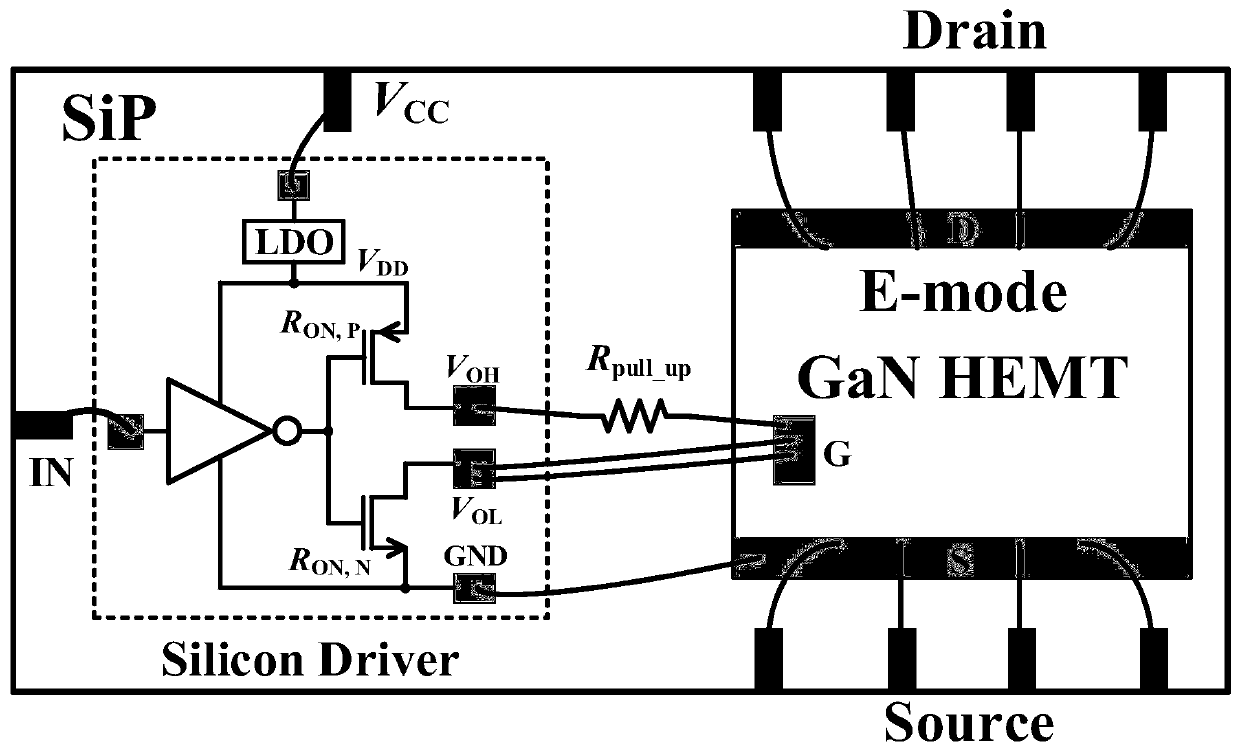
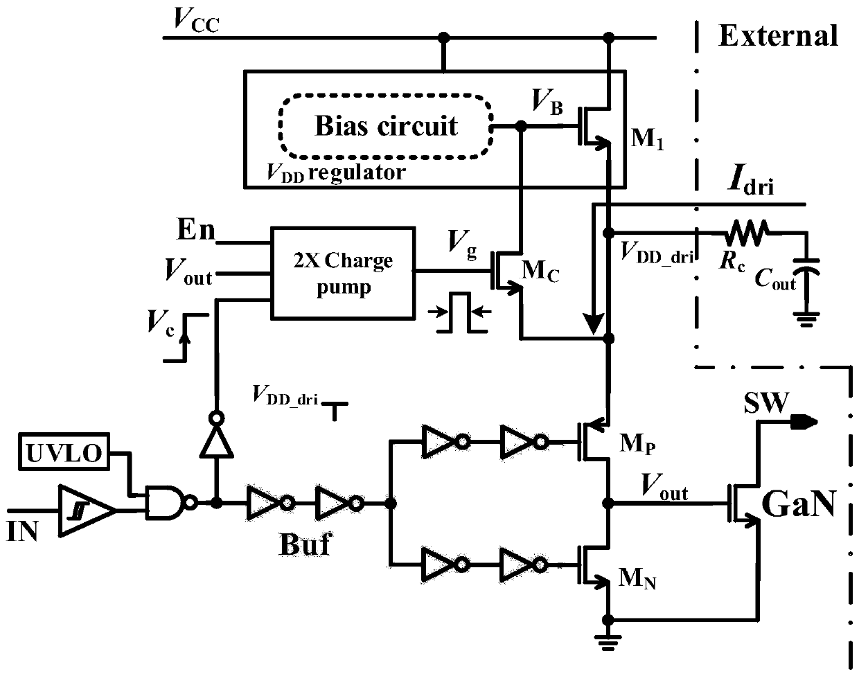
[0045] A GaN power tube gate drive circuit with controllable turn-on rate proposed by the present invention includes an internal power generation module, a gate drive module, a charge pump module, and an external capacitor C out and current limiting resistor R C , where the internal power generation module, gate drive module and charge pump module are integrated in the chip, and the external capacitor C out and current limiting resistor R C It is arranged outside the chip, which solves the problem that the gate driver and GaN power tube are mixed in the traditional SiP package, so that the current limiting resistor is fixed inside the package and cannot be adjusted freely.

[0046] The internal power generation module is used to generate the first power supply V for powering the gate drive module DD_dri , the first power supp...


PUM


Abstract

A GaN power tube gate drive circuit with a controllable opening rate comprises an internal power supply generation module, a gate drive module, a charge pump module, an external capacitor and a current-limiting resistor. The gate drive module controls charging and discharging of a GaN power tube gate according to an external control signal; a plug-in capacitor is connected with the power supply end of the gate drive module through the current-limiting resistor. The internal power supply generation module comprises a power adjusting tube controlled by the charge pump module; before the GaN power tube is conducted, the charge pump module controls the power adjusting tube to be disconnected, so the first power supply generated by the internal power supply generation module is disconnected from the power supply end of the gate driving module, only the plug-in capacitor supplies power to the gate driving module, and the gate charging rate of the GaN power tube is reduced; when the GaN powertube is switched on and after set time delay, the charge pump module controls the power adjusting tube to be switched on, so the first power supply is connected to the power supply end of the gate driving module, the first power supply and the plug-in capacitor jointly supply power to the gate driving module, and the gate charging rate of the GaN power tube is increased.

Description

technical field [0001] The invention belongs to the technical field of power device gate drive, and relates to a GaN power tube gate drive circuit with controllable turn-on rate. Background technique [0002] Compared with traditional silicon power devices, GaN transistors are a good solution for designing power converters with high frequency and high power density due to their smaller parasitic capacitance and higher conductivity. However, with the continuous improvement of the operating frequency of the chip, the fast switching operation of the GaN power tube under the condition of high voltage (600V) will introduce a large current change rate di / dt and voltage change rate dv / dt to the chip, resulting in EMI (Electromaganetic Interference) is the problem of electromagnetic interference, which seriously affects the performance of related systems such as automobiles or consumer electronics. [0003] Traditional driver chips limit the charging current by using a suitable res...

Claims


Application Information

Patent Timeline
IPC IPC(8): H02M1/08H02M1/44
CPCH02M1/08H02M1/44H02M1/0006Y02B70/10
Inventor 明鑫李相骏张波张永瑜王卓
Owner UNIV OF ELECTRONIC SCI & TECH OF CHINA
Why Eureka
Try Eureka