Image display device, quantum dot light-emitting diode and manufacturing method thereof

A technology of quantum dot light emission and manufacturing method, which is applied in semiconductor/solid-state device manufacturing, semiconductor devices, electrical components, etc., and can solve problems such as large leakage current of devices and changes in charge mobility

Active Publication Date: 2020-08-28
合肥福纳科技有限公司
View PDF7 Cites 0 Cited by
  • Summary
  • Abstract
  • Description
  • Claims
  • Application Information

AI Technical Summary

Problems solved by technology

Among them, the factor of charge injection imbalance may be that the charge mobility of the electron tran

Method used


Image

  • Image display device, quantum dot light-emitting diode and manufacturing method thereof
  • Image display device, quantum dot light-emitting diode and manufacturing method thereof

Examples


Embodiment 1

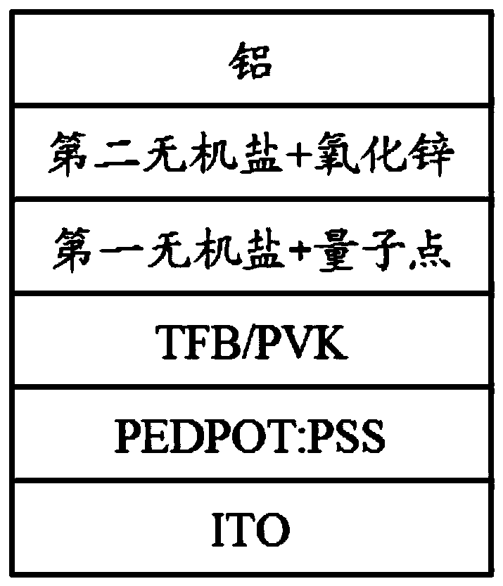
[0081] 1. Raw material preparation

[0082] 1) NaHCO 3 Solution and NaBH 4 Preparation of the solution:

[0083] Take 20mg of NaHCO 3 Disperse in 4ml ethyl acetate and stir evenly to form a uniform and transparent solution for later use;

[0084] Take 20mg of NaBH 4 Disperse in 4ml of ethanol and stir to form a uniform and transparent solution for later use.

[0085] 2) NaHCO 3 The solution is mixed with CdSe / ZnS red quantum dots, NaBH 4 The solution is mixed with ZnO nanoparticle ink:

[0086] Take 1ml of prepared NaHCO 3 The solution and 3ml of CdSe / ZnS red quantum dot ink (concentration: 30mg / ml, ink reagent: octane) are uniformly mixed at room temperature to form a homogeneous solution (quantum dot ink) and then used;

[0087] Take 1ml of NaBH with a good concentration 4 The solution and 3ml of ZnO ink (concentration: 40mg / ml, ink reagent: ethanol) are uniformly mixed at room temperature to form a uniform solution (electronic transmission ink) for use.

[0088] 3) Hole transport layer...

Embodiment 2

[0103] 1. Raw material preparation

[0104] 1) NaHSO 3 Solution and NaBH 4 Preparation of the solution:

[0105] Take 20mg of NaHSO 3 Disperse in 4ml ethyl acetate and stir evenly to form a uniform and transparent solution for later use;

[0106] Take 20mg of NaBH 4 Disperse in 4ml of ethanol and stir to form a uniform and transparent solution for later use.

[0107] 2) NaHSO 3 The solution is mixed with CdSe / ZnS red quantum dots, NaBH 4 The solution is mixed with ZnO nanoparticle ink:

[0108] Take 1ml of prepared NaHSO 3 The solution and 3ml of CdSe / ZnS red quantum dot ink (concentration: 30mg / ml, ink reagent: octane) are uniformly mixed at room temperature to form a homogeneous solution (quantum dot ink) and then used;

[0109] Take 1ml of NaBH with a good concentration 4 The solution and 3ml of ZnO ink (concentration: 40mg / ml, ink reagent: ethanol) are uniformly mixed at room temperature to form a uniform solution (electronic transmission ink) for use.

[0110] 3) Hole transport layer...


PUM

PropertyMeasurementUnit
Concentrationaaaaaaaaaa

Abstract

The invention discloses an image display device, a quantum dot light-emitting diode and a manufacturing method thereof, and belongs to the field of display equipment. The quantum dot light-emitting diode includes an anode layer, a hole transport layer, a quantum dot light-emitting layer, an electron transport layer and a cathode layer, wherein the hole transport layer formed on the anode; the quantum dot light-emitting layer is formed on the hole transport layer and contains quantum dots and a first inorganic salt, and the first inorganic salt comprises bicarbonate and/or hydrosulfite; the electron transport layer is formed on the quantum dot light-emitting layer and contains metal oxide and borohydride; and the cathode layer is formed on the electron transport layer. The quantum dot light-emitting diode can achieve improved device efficiency and lifetime through processing.

Description

Technical field [0001] This application relates to the field of display devices, and specifically to an image display device, a quantum dot light-emitting diode and a manufacturing method thereof. Background technique [0002] As the next generation of new display technology, quantum dot display technology has attracted much attention. In recent years, quantum dot display technology has been steadily advancing gradually to the stage of commercial application. Among them, the photo-induced film has entered mature commercial applications. However, what the industry is really pursuing is electro-induced (self-driving) display technology. [0003] Quantum dots have the advantages of narrow emission spectrum, adjustable color, high photochemical stability, and long fluorescence lifetime. Quantum Dot Light Emitting Diode (QLED) based on quantum dots has more outstanding efficiency and color purity than the already industrialized organic light emitting diodes (Organic Light Emitting Di...

Claims


Application Information

Patent Timeline
IPC IPC(8): H01L51/50H01L51/56
CPCH10K71/12H10K71/15H10K50/115H10K50/166
Inventor 翁兴焕蒋畅乔之勇
Owner 合肥福纳科技有限公司
Why Eureka
Try Eureka